ICST MK2772-01S, MK2772-01STR Datasheet

MK2772-01
ICRO
C
LOCK
Description
The MK2772-01 is a low cost, low jitter, high
performance VCXO and clock synthesizer for settop boxes. The on-chip Voltage Controlled
Crystal Oscillator accepts a 0 to 3V input voltage
to cause the output clocks to vary by ±100 ppm.
Using MicroClock’s patented VCXO and analog
Phase-Locked Loop (PLL) techniques, the device
uses an inexpensive 13.5 MHz crystal input to
produce multiple output clocks. All clocks are
frequency locked to the 27.00MHz output (and to
each other) with zero ppm error. The MK2772
includes a glitch-free multiplexer to switch input
sources during operation.
MicroClock manufactures the largest variety of
Set-Top Box and multimedia clock synthesizers
for all applications. Consult MicroClock to
eliminate VCXOs, crystals and oscillators from
your board.
VCXO and Set-Top Clock Source
Features
• Packaged in 20 pin SOIC
• Uses an inexpensive 13.5 MHz crystal
• On-chip VCXO (patented) with pull range
of 200ppm (minimum)
• Ability to switch input sources “on-the-fly”
• VCXO tuning voltage of 0 to 3V
• Zero ppm synthesis error (patented) in all
clocks. All exactly track 27MHz VCXO
• All clocks are frequency locked. All will vary the
same amount (in ppm) as the VCXO
• Selectable Audio clock for 256x, 384x, and 512x.
• 25mA output drive capability at TTL levels
• Advanced, low power, sub-micron CMOS process
• 5V operating voltage
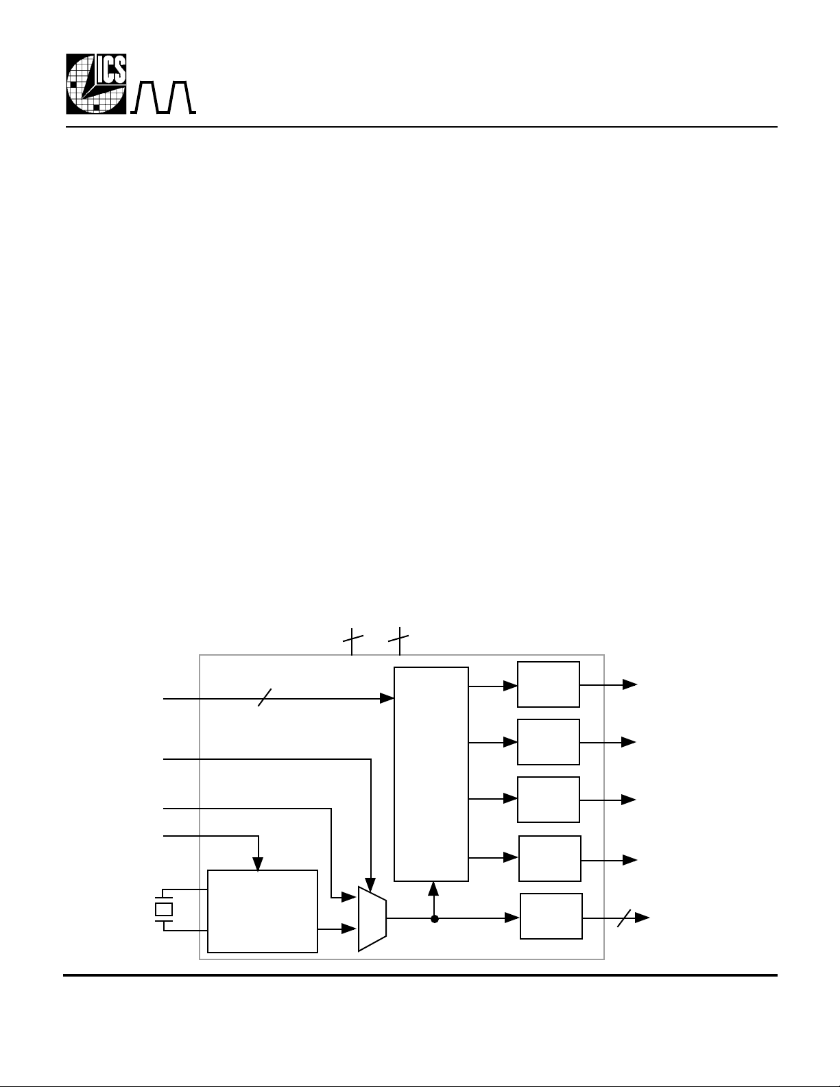
Block Diagram
ACS1:0
INMUXSEL
EXTCLKIN
VIN
13.5 MHz
pullable
crystal
MDS 2772-01 B 1 Revision 012098 Printed 11/16/00
Integrated Circuit Systems, Inc.•525 Race Street•San Jose•CA•95126•(408)295-9800tel•www.icst.com
X1
Voltage Controlled
X2
2
Crystal Oscillator
and x2 PLL
VDD
GND
33
Clock
Synthesis
Circuitry
deglitched
mux
Output
Buffer
Output
Buffer
Output
Buffer
Output
Buffer
Output
Buffers
Audio Clock
16.6667 MHz
11.0592 MHz
3.6864 MHz
3
27.000 MHz

MK2772-01
Pin Assignment
ACS1
X2
X1
VDD
VIN
VDD
GND
16.67M
1
2
3
4
5
6
7
8
93.68M
10
ICRO
20
19
18
17
16
15
14
13
12
11
C
LOCK
ACS0
EXTCLKIN
27M
GND
27M
VDD
GND
27M
11.06M
INMUXSELACLK
VCXO and Set-Top Clock Source
Audio Clock Select
ACS1 ACS0 ACLK (MHz)
0 0 8.192
0 M 16.384
0 1 11.2896
M 0 16.9344
M M 22.5792
M 1 18.432
1 0 12.288
1 M 24.576
1 1 5.6448
Input Source Select
INMUXSEL 27 MHz Input
0 EXTCLKIN
1 Internal VCXO
Pin Descriptions
Number Name Type Description
1 ACS1 TI Audio Clock Select 1. Determines ACLK frequency, as per table above.
2 X2 X Crystal connection. Connect to a pullable 13.5 MHz crystal.
3 X1 X Crystal connection. Connect to a pullable 13.5 MHz crystal.
4 VDD P Connect to +5V, and other VDDs.
5 VIN VI Voltage Input to VCXO. Zero to 3V signal which controls the frequency of the VCXO.
6 VDD P Connect to +5V.
7 GND P Connect to ground.
8 16.67M O 16.6667 MHz processor clock output.
9 3.68M O 3.6864 MHz clock output.
10 ACLK O Audio Clock Output determined by ACS1,0. Per table above.
11 INMUXSEL I Input Multiplexer Select. Selects either the internal VCXO/PLL output, or the clock on pin 19.
12 11.06M O 11.0592 MHz clock output.
13 27M O 27.00 MHz clock output.
14 GND P Connect to ground.
15 VDD P Connect to +5V.
16 27M O 27.00 MHz clock output.
17 GND P Connect to ground.
18 27M O 27.00 MHz clock output.
19 EXTCLKIN I External Clock Input. Connect an external 27 MHz clock to this pin for glitch free switching.
20 ACS0 TI Audio Clock Select 0. Determines ACLK frequency, as per table above.
Key: I = Input, TI = tri-level input, VI = VCXO input, O = output, P = power supply connection, X = crystal connection
MDS 2772-01 B 2 Revision 012098 Printed 11/16/00
Integrated Circuit Systems, Inc.•525 Race Street•San Jose•CA•95126•(408)295-9800tel•www.icst.com
 Loading...