ICST MK2771-13STR, MK2771-13S Datasheet

MK2771-13
VCXO and Set-Top Clock Source
Description
The MK2771-03 is a low cost, low jitter, high
performance VCXO and clock synthesizer
designed for set-top boxes. The on-chip Voltage
Controlled Crystal Oscillator accepts a 0 to 3V
input voltage to cause the output clocks to vary by
±100 ppm. Using ICS/MicroClock’s patented
VCXO and analog Phase-Locked Loop (PLL)
techniques, the device uses an inexpensive
13.5 MHz crystal input to produce multiple
output clocks including a selectable processor
clock, a selectable audio clock, a fixed 33.33 MHz
or 24.576 MHz, two low skew copies of the
27MHz, and a fixed 13.5 MHz. All clocks are
frequency locked to the 27.00MHz output (and to
each other) with zero ppm error, so any output can
be used as the VCXO output.
This chip directly replaces the MK2771-03 when a
13.5 MHz input crystal is substituted for the
14.31818 MHz used on the -03. Additionally, the
-13 adds 25 MHz to the processor clock selection,
and 24.576 MHz on the BCLK.
Features
• Packaged in 20 pin SOIC
• Pin for pin and functional upgrade to MK2771-03
• Ideal for systems using Oak’s MPEG decoders
• On-chip patented VCXO with pull range
of 200ppm
• VCXO tuning voltage of 0 to 3V
• Processor frequency of 16.67 MHz, 20 MHz,
25 MHz, 32 MHz, 40 MHz, or 50 MHz
• Audio clocks of 8.192, 11.2896, and 12.288 MHz
• Zero ppm synthesis error in all clocks (all exactly
track 27MHz VCXO) - patented
• Uses an inexpensive 13.5 MHz crystal
• 25mA output drive capability at TTL levels
• Advanced, low power, sub-micron CMOS process
• 5V operating voltage
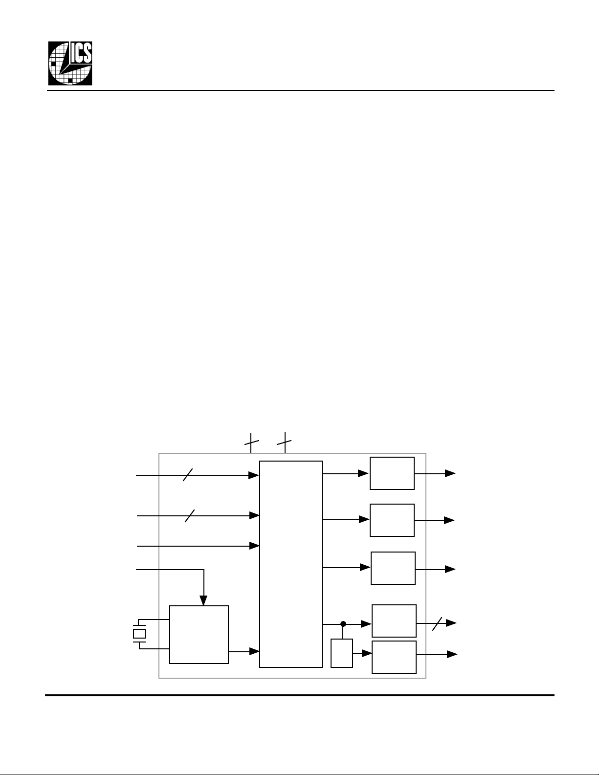
Block Diagram
PCS1:0
ACS1:0
BCS
VIN
13.5 MHz
pullable
crystal
MDS 2771-13 A 1 Revision 110298 Printed 11/16/00
Integrated Circuit Systems • 525 Race Street•San Jose•CA•95126•(408)295-9800tel•www.icst.com
X1
X2
2
2
Voltage
Controlled
Crystal
Oscillator
VDD GND
33
Clock
Synthesis
Circuitry
÷ 2
Output
Buffer
Output
Buffer
Output
Buffer
Output
Buffers
Output
Buffer
Processor Clock
Audio Clock
33.3 MHz or
24.576 MHz
2
27.000 MHz
13.500 MHz

MK2771-13
VCXO and Set-Top Clock Source
Pin Assignment
PCS0
X2
X1
VDD
VIN
VDD
GND
PCLK
ACLK
1
2
3
4
5
6
7
8
9BCLK
10
20
19
18
17
16
15
14
13
12
11
ACS1
ACS0
BCS
GND
27M
VDD
GND
27M
PCS1
13.5M
Processor Clock Select Table
PCS1 PCS0 PCLK (MHz)
0 0 50.000
0 1 16.667
M 0 25.000
M 1 32.000
1 0 40.000
1 1 20.000
0 = connect directly to ground, 1 = connect directly
to VDD, M = leave floating or unconnected
Audio Clock Table
ACS1 ACS0 ACLK (MHz)
0 0 8.192
0 1 11.2896
1 0 12.288
1 1 5.6448
Bus Clock Table
BCS BCLK (MHz)
0 33.333
1 24.576
Pin Descriptions
Number Name Type Description
1 PCS0 I Processor Clock Select 0. Selects PCLK on pin 8. See table above.
2 X2 XO Crystal connection. Connect to a pullable 13.5 MHz crystal.
3 X1 XI Crystal connection. Connect to a pullable 13.5 MHz crystal.
4, 6, 15 VDD P Connect to +5V.
5 VIN I Voltage Input to VCXO. Zero to 3V signal which controls the frequency of the VCXO.
7, 14, 17 GND P Connect to ground.
8 PCLK O Processor clock output determined by status of PCS1,0. See table above.
9 BCLK O 33.33MHz or 24.576 MHz Bus Clock output. See table above.
10 ACLK O Audio clock output determined by status of ACS1,0. See table above.
11 13.5M O 13.5 MHz clock output. Divide by two of the 27MHz VCXO output.
12 PCS1 TI Processor Clock Select 1. Selects PCLK on pin 8. See table above.
13 27M O 27.00 MHz VCXO clock output.
16 27M O 27.00 MHz VCXO clock output.
18 BCS P Bus Clock Select . Selects BCLK on pin 9. See table above.
19 ACS0 I Audio Clock Select 0. Selects ACLK on pin 10. See table above.
20 ACS1 I Audio Clock Select 1. Selects ACLK on pin 10. See table above.
Key: I = Input, TI = Tri-level input, O = output, P = power supply connection
MDS 2771-13 A 2 Revision 110298 Printed 11/16/00
Integrated Circuit Systems • 525 Race Street•San Jose•CA•95126•(408)295-9800tel•www.icst.com
 Loading...