ICST MK2731-04S, MK2731-04STR Datasheet

PRELIMINARY INFORMATION
compatible with every popular audio DAC
• Zero ppm synthesis error
• 25 mA output drive capability at TTL levels
• Advanced, low power, sub-micron CMOS process
MK2731-04C
MPEG Audio Clock
Description
The MK2731-04 is a low cost, low jitter, high
performance clock synthesizer designed to replace
expensive discrete clock oscillators in MPEG audio
applications. Using ICS/MicroClock’s patented
analog/digital Phase-Locked Loop (PLL)
techniques, the device uses an inexpensive
14.4 MHz crystal input to produce all of the
popular audio sampling frequencies.
ICS manufactures the largest variety of Set-Top
Box and multimedia clock synthesizers for all
applications. Consult ICS to eliminate VCXOs,
crystals and oscillators from your board.
Features
• Packaged in 16 pin narrow SOIC
• Replaces multiple oscillators
• 3.3V or 5V operation
• Uses an inexpensive 14.4 MHz crystal
• Supports 32 kHz, 44.1 kHz, 48 kHz, and 96 kHz
audio sampling rates
• Has 256x, 384x, and 512x sampling rates -
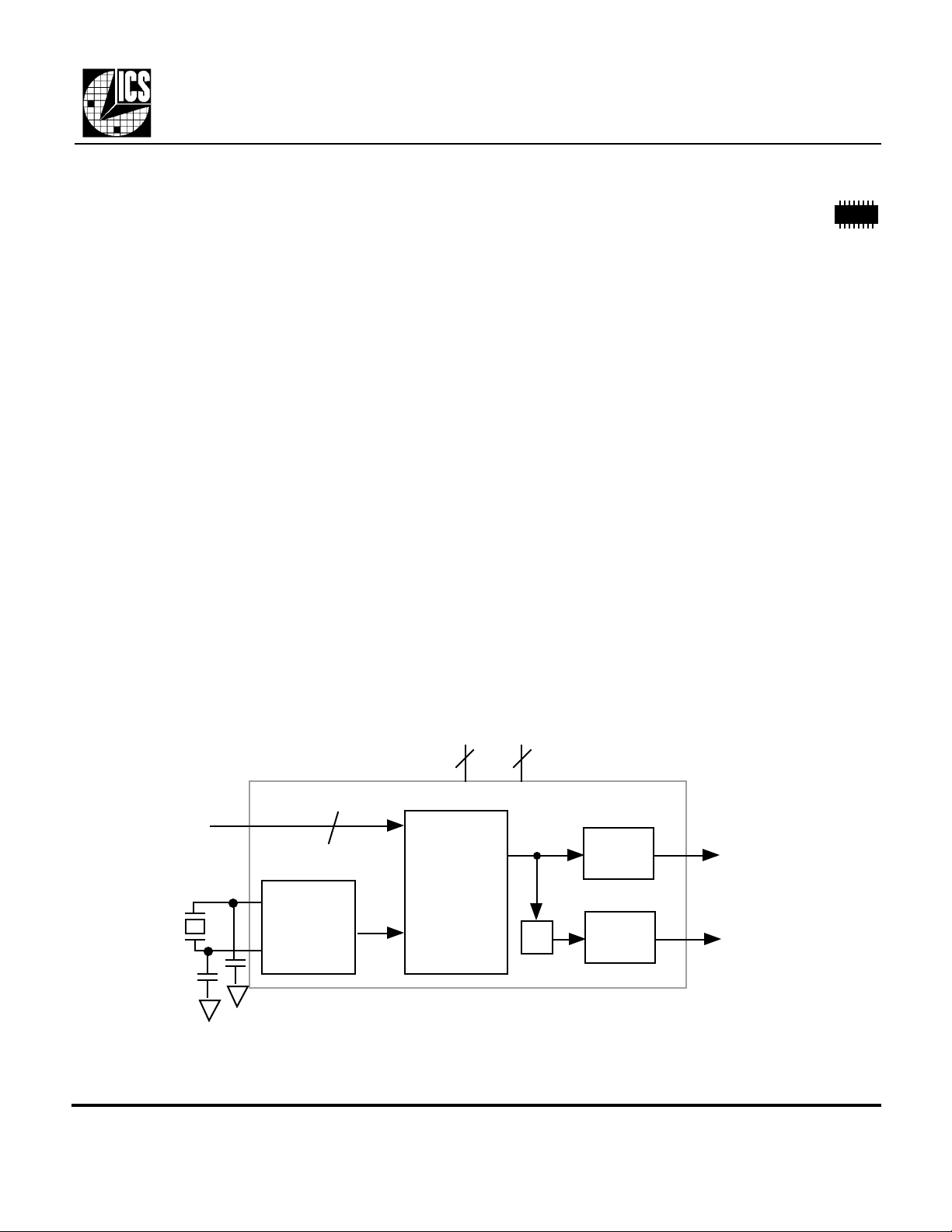
Block Diagram
3
S2:S0
X1
14.40 MHz
crystal
X2
MDS 2731-04 CA 1 Revision 122799 Printed 11/16/00
Integrated Circuit Systems, Inc. • 525 Race Street • San Jose • CA • 95126 • (408)295-9800tel • www.icst.com
Crystal
Oscillator
VDD GND
3 3
PLL/Clock
Synthesis
Circuitry
÷ 2
Output
Buffer
Output
Buffer
CLK2
CLK1

PRELIMINARY INFORMATION
MK2731-04C
MPEG Audio Clock
Pin Assignment
Output Clocks Select Table (MHz)
MK2731-04
16
X2
X1
VDD
VDD
GND
GND
GND
S2
1
2
3
4
5
6
7
8
16 pin narrow (150 mil) SOIC
15
14
13
12
11
10
DC
DC
S0
S1
DC
CLK2
VDD
CLK1
9
S2 S1 S0 CLK1 CLK2
Pin 8 Pin 13 Pin 14 Pin 9 Pin 11
0 0 0 16.9344 33.8688
0 0 1 11.2896 22.5792
0 1 0 8.192 16.384
0 1 1 18.432 36.864
1 0 0 11.2896 22.5792
1 0 1 12.288 24.576
1 1 0 Test Test
1 1 1 Test Test
Key: 0 = connect directly to GND
1 = connect directly to VDD
Pin Descriptions
Number Name Type Description
1 X2 XO Crystal connection. Connect to a parallel mode 14.4 MHz crystal.
2 X1 XI Crystal connection. Connect to a parallel mode 14.4 MHz crystal.
3, 4, 10 VDD P Connect to +3.3V or +5V. Must be same at all VDDs.
5, 6, 7 GND P Connect to ground.
8 S2 I Frequency select pin 2. Determines clock outputs per table above.
9 CLK1 O Clock output 1 set by status of S0-S2. See table above. This output is CLK2/2
11 CLK2 O Clock output 2 set by status of S0-S2. See table above.
12, 15, 16 DC - Don't Connect. Do not connect anything to these pins.
13 S1 I Frequency select pin 1. Determines clock outputs per table above.
14 S0 I Frequency select pin 0. Determines clock outputs per table above.
Key: I = Input with internal pull-up resistor; O = output; P = power supply connection; XI, XO = crystal
connections
External Components
The MK2731-04 requires a minimum number of external components for proper operation. Decoupling
capacitors of 0.01µF should be connected between VDD and GND on pins 3 and 5, and VDD and GND
on pins 10 and 6, as close to the MK2731-04 as possible. Other VDDs can be connected to pin 10. A series
termination resistor of 33 Ω may be used for each clock output. Any unused clock outputs should be left
unconnected (DC, floating). The input crystal must be connected as close to the chip as possible. The input
crystal should be fundamental mode, parallel resonant. For accurate outputs, the crystal should be tuned
with two identical capacitors to ground, as shown on the block diagram. The value of these two crystal caps
should be equal to (CL-6)*2, where CL is the crystal load (or correlation) capacitance.
MDS 2731-04 CA 2 Revision 122799 Printed 11/16/00
Integrated Circuit Systems, Inc. • 525 Race Street • San Jose • CA • 95126 • (408)295-9800tel • www.icst.com
 Loading...