ICST MK2731-03STR Datasheet

MK2731-03C
MPEG Audio Clock Synthesizer
Description
The MK2731-03 is a low cost, low jitter, high
performance PLL clock synthesizer designed to
replace oscillators and PLL circuits in set-top box
and multimedia systems. Using our proprietary
analog Phase-Locked Loop (PLL) techniques, the
device uses an inexpensive crystal or clock input to
produce up to three output clocks. All of the audio
frequencies are synthesized exactly, with zero ppm
error, and locked to the 27 MHz clock.
MicroClock manufactures the largest variety of
Set-Top Box and multimedia clock synthesizers
for all applications. Consult MicroClock to
eliminate VCXOs, crystals and oscillators from
your board.
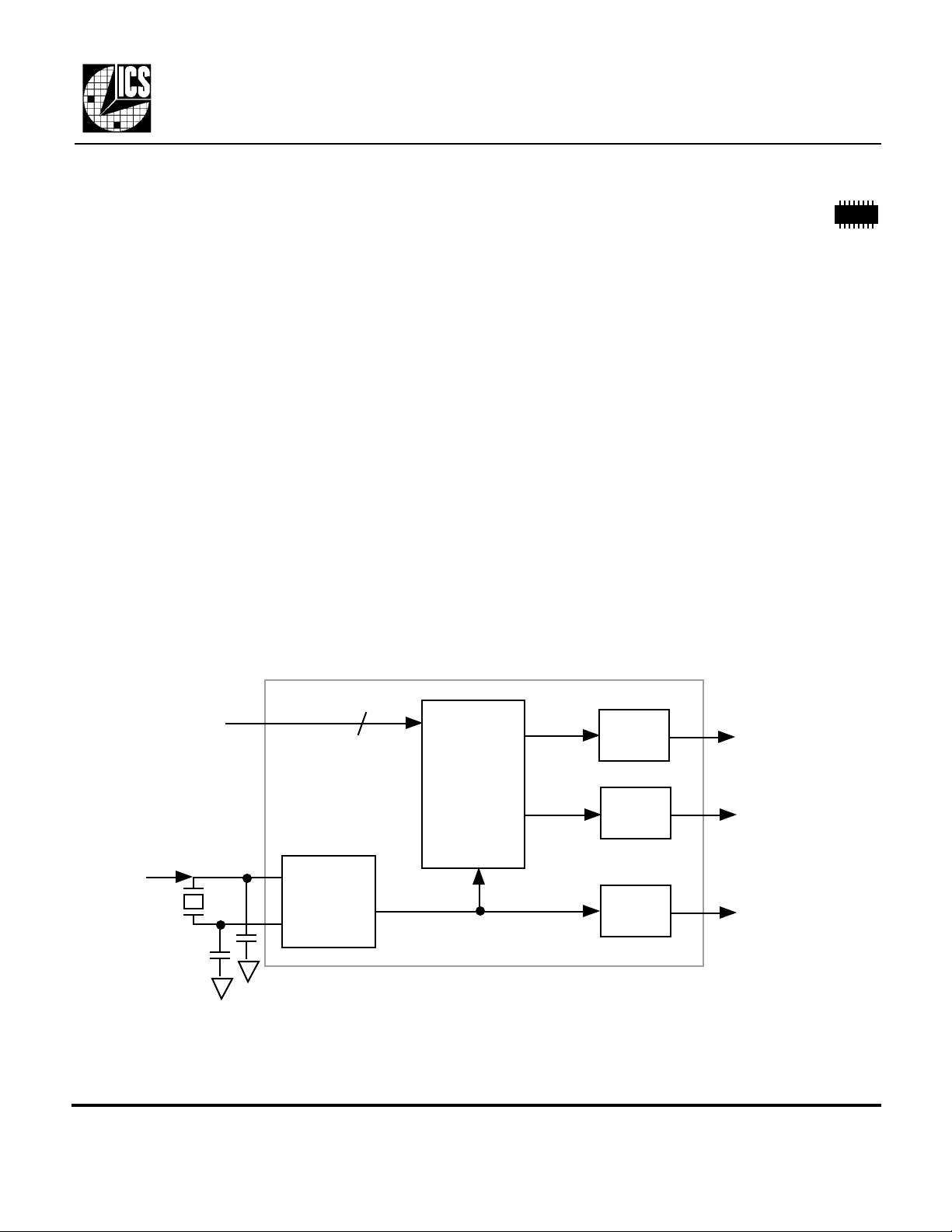
Block Diagram
Features
• Packaged in 16 pin narrow SOIC
• Produces exact audio clocks from the video
• Uses a crystal or clock input
• Zero ppm synthesis error in all clocks
• All frequencies are frequency locked
• 25mA output drive capability at TTL levels
• Advanced, low power, sub-micron CMOS process
• 3.3V or 5V operating voltage
Crystal
3
PLL/Clock
Synthesis
Circuitry
Output
Buffer
Output
Buffer
Output
Buffer
CLK1
CLK2
REF
S2:0
27 MHz crystal
or clock
(Capacitors are required
for crystal tuning)
MDS 2731-03C D 1 Revision 011101
Integrated Circuit Systems, Inc.• 525 Race Street, San Jose, CA, 95126 • (408) 295-9800 tel • www.icst.com
X1
Oscillator
X2

Pin Assignment
MK2731-03C
MPEG Audio Clock Synthesizer
MK2731-03C
Output Clock Select Table (MHz)
16
X2
X1
VDD
VDD
GND
GND
S2
GND
1
2
3
4
5
6
7
8
16 pin narrow (150 mil) SOIC
Pin Descriptions
Number Name Type Description
1 X2 XO Crystal connection to a 27 MHz fundamental crystal. Leave unconnected for clock input.
2 X1 XI Crystal connection to a 27 MHz fundamental crystal. Can also be connected to input clock.
3 VDD P VDD. Connect to VDD.
4 VDD P VDD. Connect to VDD.
5 GND P Connect to ground.
6 GND P Connect to ground.
7 S2 I Clock Select 2. Selects outputs per table above.
8 GND P Connect to ground.
9 DC - Do not connect anything to this pin.
10 CLK1 O Clock output 1 determined by status of S2, S1, S0. See table above.
11 S1 I Clock Select 1. Selects outputs per table above.
12 NC - No Connect. Nothing is connected internally to this pin.
13 S0 I Clock Select 0. Selects outputs per table above.
14 CLK2 O Clock output 2 determined by status of S2, S1, S0. See table above.
15 NC - No Connect. Nothing is connected internally to this pin.
16 REF O Reference crystal output or off. See table above.
15
14
13
12
11
10
REF
NC
CLK2
S0
NC
S1
CLK1
DC
9
Input S2 S1 S0 CLK1 CLK2 REF
27 0 0 0 Off 8.192 Off
27 0 0 1 Off 11.2896 Off
27 0 1 0 Off 12.288 Off
27 0 1 1 Off 24.576 Off
27 1 0 0 4.096 8.192 27
27 1 0 1 5.6448 11.2896 27
27 1 1 0 6.144 12.288 27
27 1 1 1 12.288 24.576 27
Key: 0 = connect pin directly to ground
1 = connect pin directly to VDD
Off = clock stopped low
Key: I = Input, O = output, P = power supply connection
MDS 2731-03C D 2 Revision 011101
Integrated Circuit Systems, Inc.• 525 Race Street, San Jose, CA, 95126 • (408) 295-9800 tel • www.icst.com
 Loading...