MK2716
ICRO
C
LOCK
Description
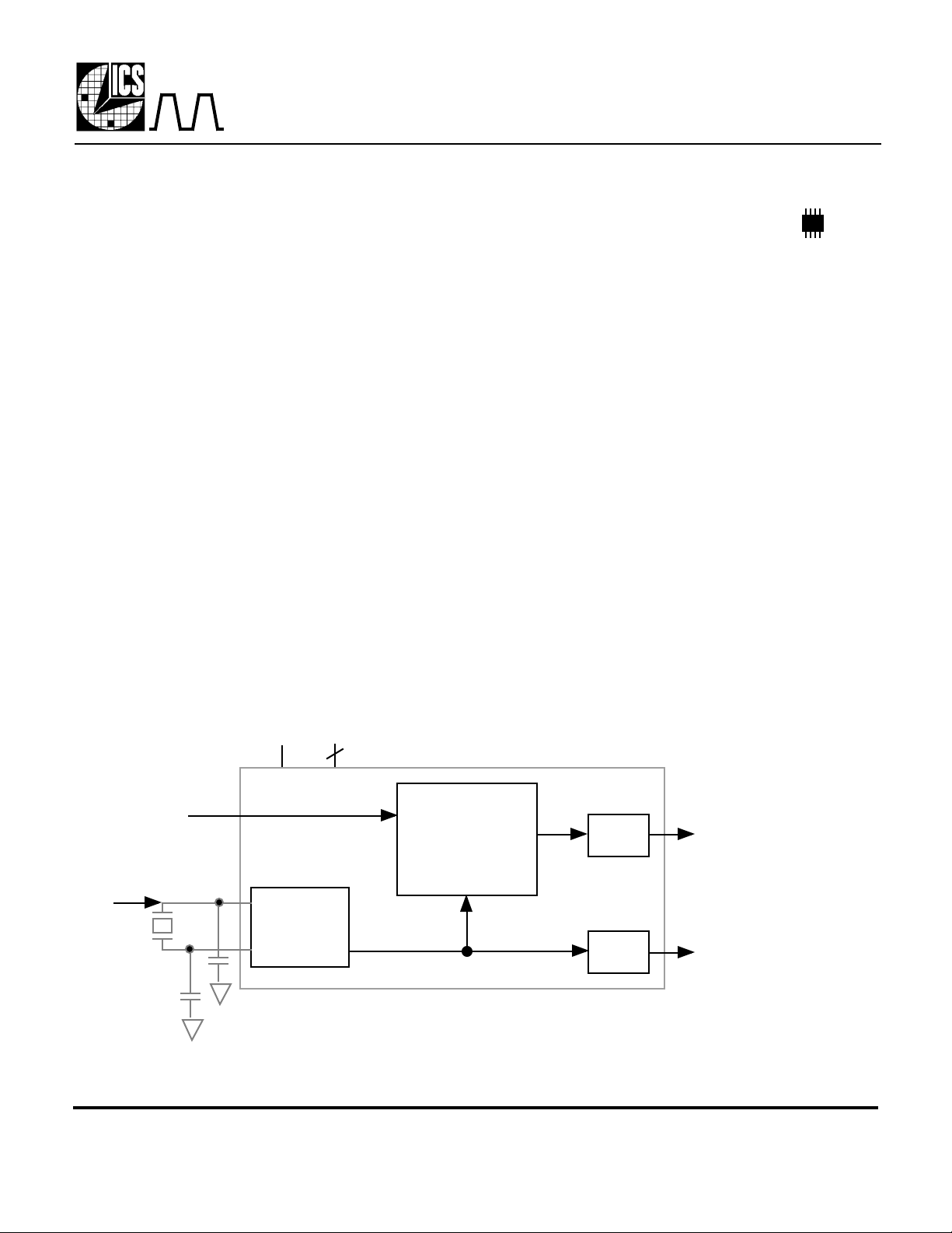
The MK2716 is a low cost, low jitter, high
performance clock synthesizer designed to
produce the 74.176 MHz and 74.25 MHz clocks
necessary for HDTV systems. Using analog PhaseLocked Loop (PLL) techniques, the device accepts
a 27 MHz clock or fundamental crystal input. The
zero ppm synthesis error exactly locks the display
to the digital stream.
MicroClock offers a wide variety of clock
synthesizers for desktop and portable computers,
and multimedia systems. Consult MicroClock to
eliminate crystals and oscillators from your board.
HDTV Clock Synthesizer
Features
• Packaged as 8 pin SOIC or die
• Input frequency of 27 MHz
• Zero ppm synthesis error in output clock
• 3.3 V or 5.0 V±10% operating supply
• 25 mA drive capability at TTL levels
• Ideal for HDTV applications and oscillator
manufacturers
• Advanced, low power CMOS process
• Custom masks easily and quickly made
Block Diagram
SEL
27 MHz
crystal or
clock
X1
X2
VDD GND
2
Clock
Buffer
Clock Synthesis
and Control
Circuitry
Output
Buffer
Output
Buffer
CLK
74.17582418 MHz or
74.2500 MHz
27.0000 MHz
MDS 2716 B 1 Revision 062599 Printed 11/16/00
MicroClock Division of ICS • 525 Race Street • San Jose • CA • 95126•(408)295-9800tel•(408)295-9818fax

MK2716
Pin Assignment
ICLK/X1
VDD
GND
CLK
1 8
2
3
4
8 pin SOIC
Pin Descriptions
ICRO
C
7
6
5
LOCK
X2
27M
SEL
GND
HDTV Clock Synthesizer
Frequency Select Table (MHz)
SEL CLK
0 74.17582418
1 74.25
Number Name Type Description
1 ICLK/X1 XI Input clock connection. Connect to a 27 MHz clock input or 27 MHz fundamental crystal.
2 VDD P Connect to +3.3V or +5V.
3 GND P Connect to ground.
4 CLK O 74.17582418 MHz or 74.25 MHz clock output (see table above).
5 GND P Connect to ground.
6 SEL I Select pin determines value of CLK per table above.
7 27M O 27 MHz buffered clock or crystal oscillator output.
8 X2 XO Connect to 27 MHz crystal, or leave unconnected for clock input.
Type: I = Input; O = output; P = power supply connection; XI, XO = crystal connections
Decoupling and External Components
The MK2716 requires a 0.1µF decoupling capacitor to be connected between VDD and GND on pins 2
and 3. It must be connected close to the MK2716. Pin 5 can be connected to pin 3. A 33 Ω terminating
resistor should be placed close to pin 4, and pin 7. If using a crystal input, it should be a 27.00 MHz,
parallel resonant, fundamental mode, with load (correlation) capacitance of 18 pF. If the crystal has a load
capacitance of 20 pF, connect 4 pF capacitors from X1 and X2 to ground.
MDS 2716 B 2 Revision 062599 Printed 11/16/00
MicroClock Division of ICS • 525 Race Street • San Jose • CA • 95126•(408)295-9800tel•(408)295-9818fax
 Loading...