MK2059-01
VCXO-Based Frame Clock Frequency Translator
Description
The MK2059-01 is a VCXO (V oltage Controlled Crystal
Oscillator) based clock generator that produces
common telecommunications reference frequencies.
The output clock is phase locked to an 8kHz (frame
rate) input reference clock. The MK2059-01 also
provides jitter attenuation. Included in the selection of
output frequencies are these common system clocks:
1.544 MHz (T1) 2.048 (E1)
19.44 MHz (OC-3) 16.384 MHz (8x E1)
This monolithic IC, combined with an external
inexpensive quartz crystal, can be used to replace a
more costly hybrid VCXO retiming module. Through
selection of external loop filter components, the PLL
loop bandwidth and damping factor can be tailored to
meet input clock jitter attenuation requirements. A loop
bandwidth down to the Hz range is possible.
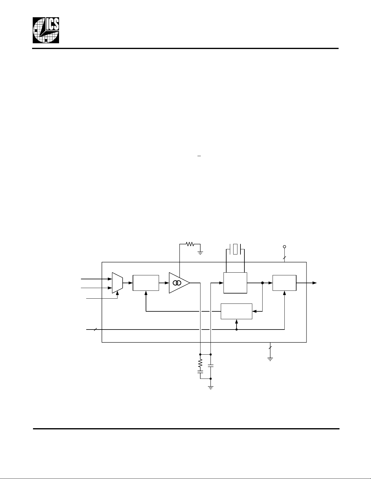
Block Diagram
Features
• Generates T1, E1, OC-3 and other common telecom
clock frequencies from an 8kHz frame clock
• Configurable jitter attenuation characterisitics,
excellent for use as a Stratum source de-jitter circuit
• 2:1 Input MUX for input reference clocks
• VCXO-based clock generation offers very low jitter
and phase noise generation
• Output clock is phase and frequency locked to the
selected input reference clock
• Fixed input to output phase relationship
• +115ppm minimum crystal frequency pullability
range, using recommended crystal
• Industrial temperature range
• Low power CMOS technology
• 20 pin SOIC package
• Single 3.3V power supply
Pullable xtal
VDD
8kHz Ref Input
8kHz Ref Input
ISEL
SEL2:0
ICLK2
ICLK1
ISET
1
0
3
Phase
Detector
Charge
Pump
CHGP
VCXO
Feedback
Divider
VIN
X2X1
GND
VDD
Output
Divider
4
3
CLK
MDS 2059-01 B 1 Revision 071001
Integrated Circuit Systems, Inc. ● 525 Race Street, San Jose, C A 95126 ● tel (408) 295-9 800 ● www.icst.com

MK2059-01
VCXO-Based Frame Clock Frequency Translator
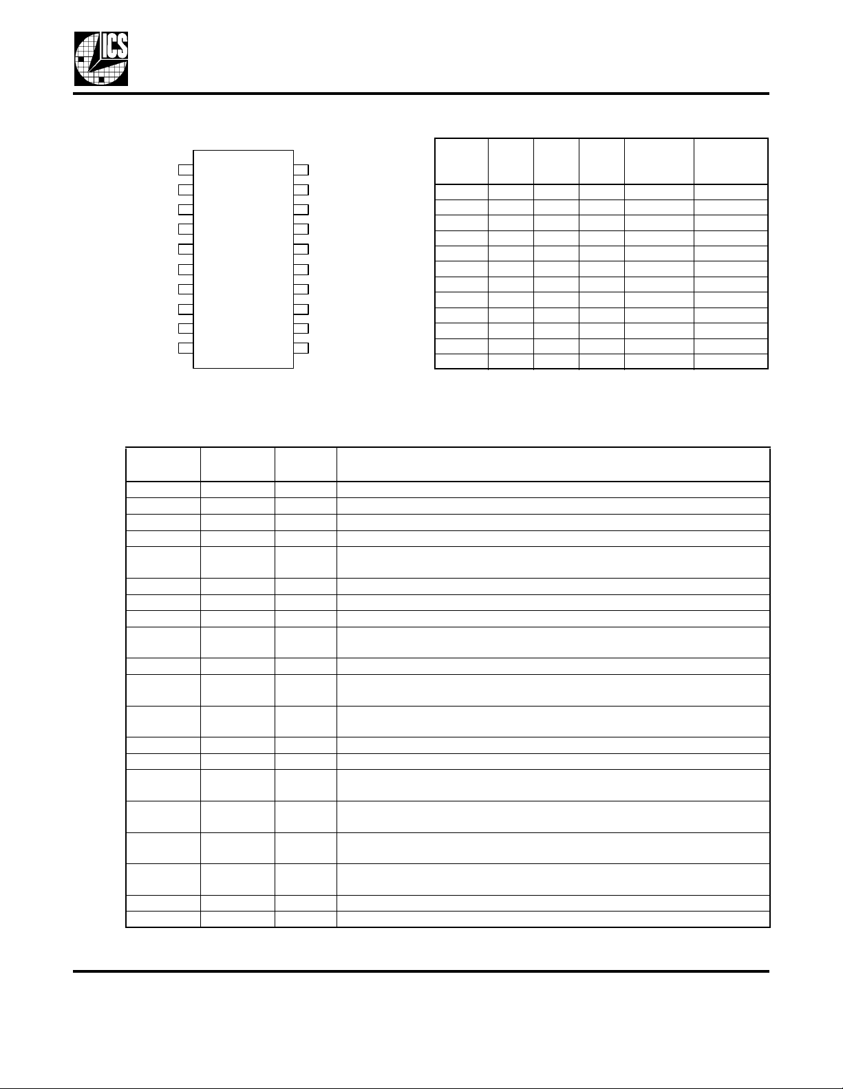
Pin Assignment
X1 X2
VDD
VDD
VDD
VIN
GND
GND
GND
CHGP
ISE T
1
2
3
4
5
6
7
8
9
10
20 pin 300 mil SOIC
Pin Descriptions
Pin
Number
1 X1 - Crystal Input. Connect this pin to the specified crystal.
2 VDD Power Power Supply. Connect to +3.3V.
3 VDD Power Power Supply. Connect to +3.3V.
4 VDD Power Power Supply. Connect to +3.3V.
5 VIN Input VCXO Control Voltage Input. Connect this pin to CHGP pin and the external
6 GND Power Connect to ground
7 GND Power Connect to ground
8 GND Power Connect to ground
9 CHGP Output Charge Pump Output. Connect this pin to the external loop filter and to pin
10 ISET - Charge pump current setting node, connection for setting resistor.
11 SEL2 Input Output Frequency Selection Pin 2. Determines output frequency as per table
12 SEL1 Input Output Frequency Selection Pin 1. Determines output frequency as per table
13 NC Input No Internal Connection.
14 CLK Output Clock Ou tput
15 SEL0 Input Output Frequency Selection Pin 0. Determines output frequency as per table
16 ICLK2 Input Input Clock Connection 2. Connect an input reference clock to this pin. If
17 ICLK1 Input Input Clock Connection 1. Connect an input reference clock to this pin. If
18 ISEL Input Input Selection. Used to select which refere nce input c lock is ac tive. Low inpu t
19 GND Power Connect to ground.
20 X2 - Crystal Output. Connect this pin to the specified crystal.
Pin
Name
20
19
18
17
16
15
14
13
12
11
Pin
Type
Output Clock Selection Table
Output
Input SEL2 SEL1 SEL0
GND
ISEL
IC L K1
IC L K2
SEL0
CLK
NC
SEL1
SEL2
8 kHz 0 0 0 1.544 24.704
8 kHz 0 0 1 2.048 24.576
8 kHz 0 1 0 16.384 16.384
8 kHz 0 1 1 17.664 17.664
8 kHz M 0 0 18.528 18.528
8 kHz M 0 1 20.00 20.00
8 kHz M 1 0 25.00 25.00
8 kHz M 1 1 25.92 25.92
8 kHz 1 0 0 19.44 19.44
8 kHz 1 0 1 20.48 20.48
8 kHz 1 1 0 24.704 24.704
8 kHz 1 1 1 24.576 24.576
Note: For SEL input pin programming:
0 = GND, 1 = VDD, M = Floating
Pin Description
loop filter as shown in this data sheet.
VIN.
above. Internally biased to VDD/2.
above. Internal pull-up.
above. Internal pull-up.
unused, connect to ground.
unused, connect to ground.
level selects ICLK1, high input level selects ICLK2. Internal pull-up.
Clock
(MHz)
Crystal
Used (MHz)
MDS 2059-01 B 2 Revision 071001
Integrated Circuit Systems, Inc. ● 525 Race St reet, San Jose, CA 9512 6 ● tel (408) 295-9800 ● www.icst.com

VCXO-Based Frame Clock Frequency Translator
MK2059-01
Functional Description
The MK2059-01 is a clock generator IC that generates
an output clock directly from an internal VCXO circuit
which works in conjunction with an external quartz
crystal. The VCXO is controlled by an internal PLL
(Phase Locked Loop) circuit, enabling the device to
perform clock regeneration from an input reference
clock. The MK2059-01 is configured to provide a MHz
communications reference clock output from an 8kHz
input clock. There are 12 selectable output
frequencies. Please refer to the Output Clock Selection
Table on Page 2.
Most typical PLL clock devices use an internal VCO
(Voltage Controlled Oscillator) for output clock
generation. By using a VCXO with an external crystal,
the MK2059-01 is able to generate a low jitter, low
phase-noise output clock within a low bandwidth PLL.
This serves to provide input clock jitter attenuation and
enables stable operation with a low frequency
reference clock.
The VCXO circuit requires an external pullable crystal
for operation. External loop filter components enable a
PLL configuration with low loop band wid th.
Application Information
Quartz Crystal
It is important that the correct type of quartz crystal is
used with the MK2059-01. Failure to do so may result
in reduced frequency pullability range, inability of the
loop to lock, or excessive output phase jitter.
The MK2059-01 operates by phase-locking the VCXO
circuit to the input signal of the selected ICLK input.
The VCXO consists of the external crystal and the
integrated VCXO oscill ator circuit. To achieve the best
performance and reliability, a crystal device with the
recommended parameters (shown bel ow) must be
used, and the layout guidelines discussed in the PCB
Layout Recommendations section must be followed.
The frequency of oscillation of a quartz crystal is
determined by its cut and by the external load
capacitance. The MK2059-01 incorporates variable
load capacitors on-chip which “pull”, or change, the
frequency of the crystal. The crystals specified for use
with the MK2059-01 are designed to have zero
frequency error when the total of on-chip + stray
capacitance is 14pF. To achieve this, the layout should
use short traces between the MK2059-01 and the
crystal.
A complete description of the recommended crystal
parameters is shown below.
Recommended Crystal Parameters:
Output Frequency Configuration
The MK2059-01 is configured to generate a set of
output frequencies from an 8kHz input clock. Please
refer to the Output Clock Selection Table on Page 2.
Input bits SEL2:0 are set according to this table, as is
the external crystal frequency. Please refer to the
Quartz Crystal section on this page regarding external
crystal requirements.
Input Mux
The Input Mux serves to select between two alternate
input reference clocks. Upon reselection of the input
clock, clock glitches on the output clock will not be
generated due to the “fly-wheel” effect of the VCXO
(the quartz crystal is a high-Q tuned circuit). When the
input clocks are not phase aligned, the phase of the
output clock will change to reflect the phase of newly
selected input at a controlled phase slope (rate of
phase change) as influenced by the PLL loop
characteristics.
MDS 2059-01 B 3 Revision 071001
Operating Temperature Range
Commercial Applications 0 to 70
Industrial Applications -40 to 85
Initial Accuracy at 25
Temperature Stability ±30 ppm
Aging ±20 ppm
Load Capacitance Note 1
Shunt Capacitance, C0 7 pF Max
C0/C1 Ratio 250 Max
Equivalent Series Resistance 35 Ω Max
Note 1: For crystal frequencies between 13.5MHz and
27MHz the nominal crystal load capacitance
specification should be 14pF. Contact ICS MicroClock
applications at (408) 297-1201 regarding the use of a
crystal below 13.5MHz.
To obtain a list of qualified crystal devices that meet
these requirements, please contact ICS MicroClock
applications department.
°C ±20 ppm
°C
°C
Integrated Circuit Systems, Inc. ● 525 Race St reet, San Jose, CA 9512 6 ● tel (408) 295-9800 ● www.icst.com
 Loading...