

ICS9250-08
Third party brands and names are the property of their respective owners.
Integrated
Circuit
Systems, Inc.
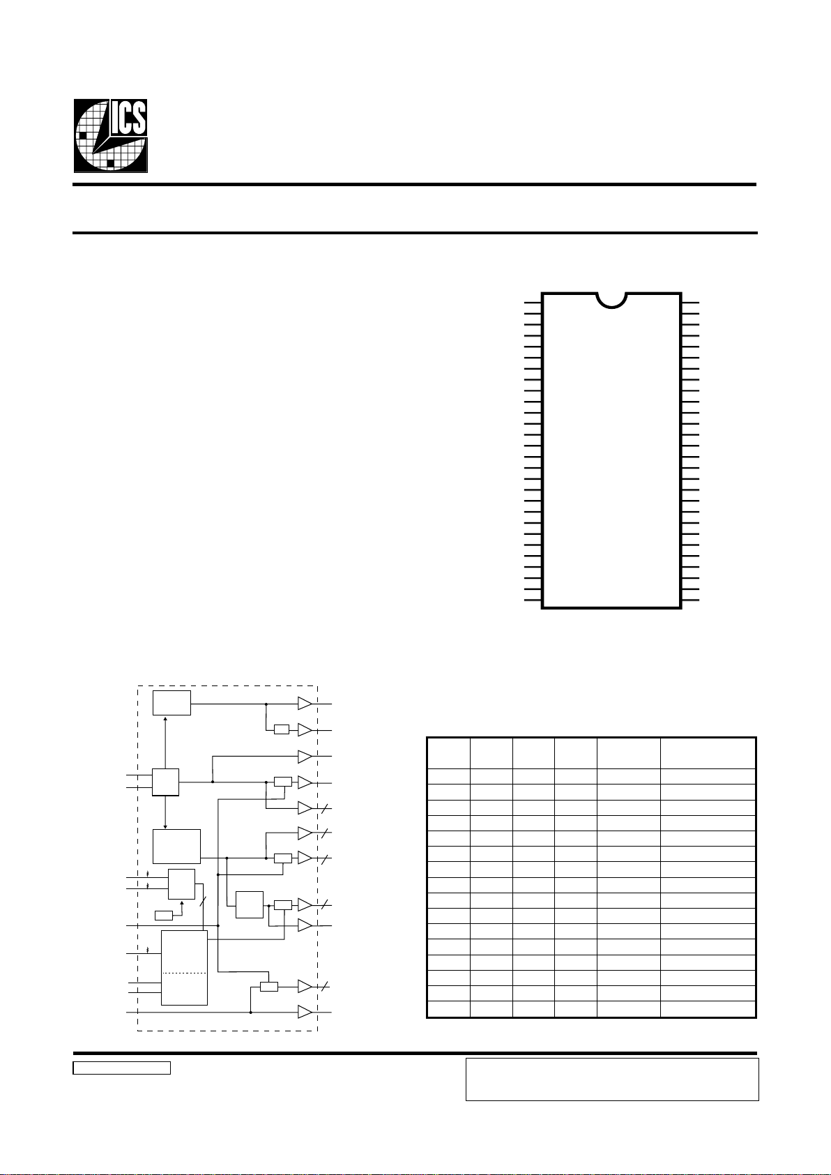
Block Diagram
Frequency Generator & Integrated Buffers for Celeron & PII/III™
9250-08 Rev H 10/8/99
Functionality
Pin Configuration
Recommended Application:
BX, Appollo Pro 133 type of chip set.
Output Features:
• 3 - CPUs @2.5V, up to 150MHz.
• 17 - SDRAM @ 3.3V, up to 150MHz.
• 7 - PCI @3.3V
• 2 - IOAPIC @ 2.5V
• 1 - 48MHz, @3.3V fixed.
• 1 - 24MHz @ 3.3V
• 2 - REF @3.3V, 14.318MHz.
Features:
• Up to 150MHz frequency support
• Support power management: CPU, PCI, stop and Power
down Mode form I
2
C programming.
• Spread spectrum for EMI control (0 to -0.5%, ± 0.25%).
• Uses external 14.318MHz crystal
Key Specifications:
• CPU – CPU: <175ps
• CPU – PCI: min = 1ns max = 4ns
• PCI – PCI: <250ps
• SDRAM - SDRAM: <500ps
56-Pin SSOP
* Internal Pull-up Resistor of 240K to 3.3V on indicated inputs
** Internal Pull-down resistor of 240K to GND on indicated inputs.
VDDREF
* REF1
*PCI_STOP/REF0
GND
X1
X2
VDDPCI
*MODE/PCICLK_F
**FS3/PCICLK0
GND
VDDPCI
BUFFERIN
SDRAM11
SDRAM10
VDDSDR
SDRAM9
SDRAM8
GND
SDRAM15
SDRAM14
GND
SDATA
SCLK
PCICLK1
PCICLK2
PCICLK3
PCICLK4
PCICLK5
FS2/
VDDLIOAPIC
IOAPIC0
IOAPIC_F
GND
CPUCLK_F
CPUCLK1
VDDLCPU
CPUCLK2
GND
CPU_STOP#
SDRAM_F
VDDSDR
SDRAM0
SDRAM1
GND
SDRAM2
SDRAM3
SDRAM4
SDRAM5
VDDSDR
SDRAM6
SDRAM7
GND
SDRAM12
SDRAM13
VDD48
24MHz/FS0*
48MHz/FS1*
ICS9250-08
1
2
3
4
5
6
7
8
9
10
11
12
13
14
15
16
17
18
19
20
21
22
23
24
25
26
27
28
56
55
54
53
52
51
50
49
48
47
46
45
44
43
42
41
40
39
38
37
36
35
34
33
32
31
30
29
{
I
C
2
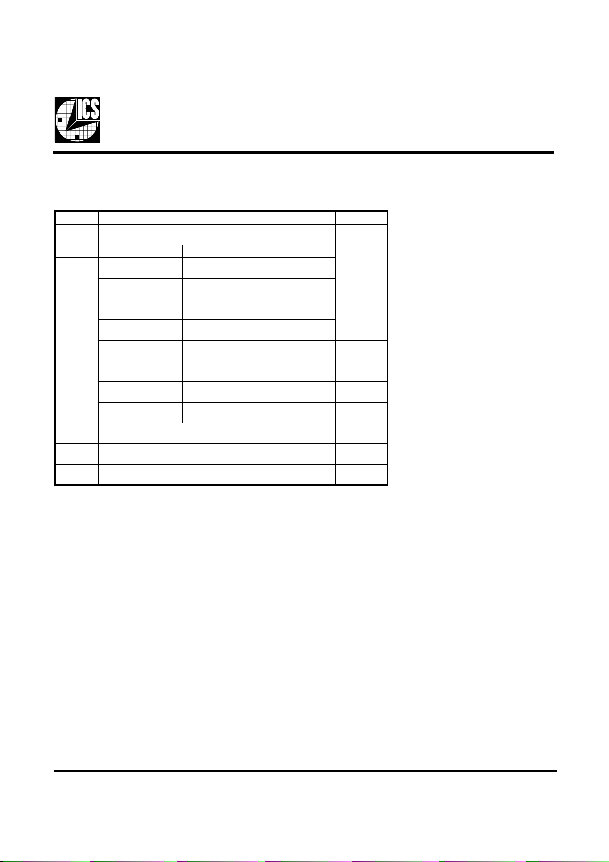
3SF2SF1SF0SF
UPC
)zHM(
)zHM(KLCICP
1111 331)4/UPC(3.33
1110 421)4/UPC(13
1101 051)4/UPC(5.73
1100 041)4/UPC(53
1011 501)3/UPC(53
1010 011)3/UPC(76.63
1001 511)3/UPC(33.83
1000 021)3/UPC(00.04
0111 3.001)3/UPC(34.33
0110 331)3/UPC(33.44
0101 211)3/UPC(33.73
0100 301)2/UPC(33.43
0011 8.66)2/UPC(04.33
0010 3.38)2/UPC(56.14
0001 57)2/UPC(5.73
0000 421)2/UPC(33.14
CPU_STOP#
PCI_STOP#
PLL2
PLL1
Spread
Spectrum
48MHz
IOAPIC0
CPUCLK [2:1]
CPUCLK_F
IOAPIC_F
SDRAM [15:0]
SDRAM_F
PCICLK [5:0]
PCICLK_F
X1
X2
XTAL
OSC
PCI
CLOCK
DIVDER
STOP
STOP
÷2
STOP
STOP
POR
SDATA
SCLK
FS[3:0]
MODE
{
I
C
2
Control
Logic
Config.
Reg.
REF [1:0]
24MHz
LATCH
1
2
2
16
66
4
BUFFERIN
ICS reserves the right to make changes in the device data identified in
this publication without further notice. ICS advises its customers to
obtain the latest version of all device data to verify that any
information being relied upon by the customer is current and accurate.
2
ICS92 50-08
Third party brands and names are the property of their respective owners.
Pin Configuration
Notes:
1: Bidirectional input/output pins, input logic levels are latched at internal power-on-reset. Use 10Kohm resistor
to program logic Hi to VDD or GND for logic low.
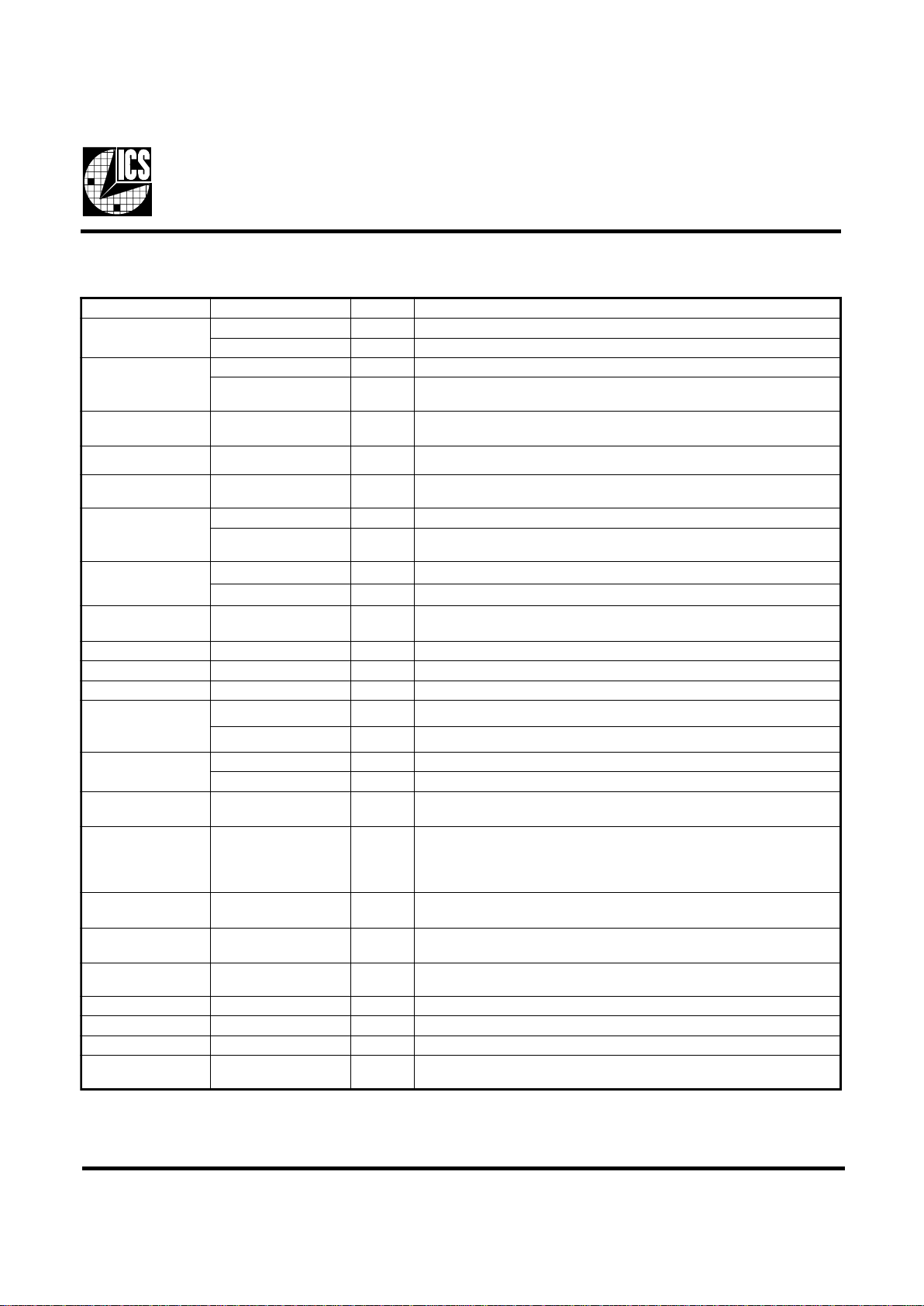
REBMUNNIPEMANNIPEPYTNOITPIRCSED
2
1FERTUOtuptuokcolcecnereferzHM813.41
2SF
1
NIICPDDVotpu-llupsaH.tupnitcelesycneuqerfdehctaL
3
0FERTUOtuptuokcolcecnereferzHM813.41
#POTS_ICP
1
NI
.wolnehwlevel"0"cigolta]0:5[KLCICPstlaH
)0=EDOM,elibomni(
,24,43,62,32,01,4
35,84
DNGRWP.dnuorG
51XNI.)Fp33lanimon(,pacdaollanretnisaH.tupnizHM813.41
62XTUO
kcabdeefdna)Fp33(pacdaollanretnisaH.tuptuolatsyrC
1Xotrotsiser
8
F_KLCICPTUO#POTS_ICPybdetceffatonkcolcSUBgninnureerF
EDOM
1
NI
nehw#POTS_ICPot3nipstrevnoC.tcelesEDOMroftupnidehctaL
.tnemeganamrewoprofwol
9
3SF
1
NInwod-llup,tupnitcelesycneuqerfdehctaL
0KLCICPTUO#POTS_ICPybdetceffatonkcolcSUBgninnureerF
11,21,31,41,61]1:5[KLCICPTUO.stuptuOkcolCICP
71NIREFFUBNIsreffuBroftupnI
72ATADSNII(.tropgifnoclairesrofniatadlaireS
2
)C
82KLCSNII(.tropgifnoclairesroftupnikcolC
2
)C
03
zHM42TUO.DFroO/IrepuSroftuptuokcolczHM42
0SF
1
NI.4DDVotpu-llupsaH.tupnitcelesycneuqerfdehctaL
92
zHM84TUO.BSUroftuptuokcolczHM84
1SF
1
NI.2DDVotpu-llupsaH.tupnitcelesycneuqerfdehctaL
,02,51,7,1
,1354,73
,FERDDV,ICPDDV
84DDV,RDSDDV
RWP.noitcnufrofspuorgrewopees,ylppusrewopV3.3lanimoN
,81,33,23,52,42
,63,53,22,12,91
,34,14,04,93,83
44
]0:51[MARDSTUOskcolcMARDS
64F_MARDSTUO#POTS_UPCybdetceffatoNkcolcMARDSgninnureerF
74#POTS_UPCNI
KLCUPCstlaH]0:51[MARDS,0CIPAOI,]1:2[
.wolnehwlevel"0"cigoltaskcolc
65,05
,UPCLDDV
CIPAOILDDV
RWP.lanimonV5.2,ylppusrewopreffubkcolcCIPAOIdnaUPC
550CIPAOITUOCIPAOILDDVybderewoP)zHM813.41(.tuptuokcolcCIPAOI
94,15]1:2[KLCUPCTUO)zHM6.66ro06(2LDDVybderewoP.skcolctuptuOUPC
25F_KLCUPCTUO.#POTS_UPCehtytdetceffatoN.kcolctuptuoUPCgninnureerF
45F_CIPAOITUO
gninnureerF.tuptuokcolcCIPAOI#POTS_UPCehtybdetceffatoN
CIPAOILDDVybderewoP)zHM81813.41(
3
ICS92 50-08
Third party brands and names are the property of their respective owners.
General Description
The ICS9250-08 is the single chip clock solution for Desktop/
designs using BX, Appollo Pro 133 type of chip sets. It provides
all necessary clock signals for such a system.
Spread spectrum may be enabled through I2C programming.
Spread spectrum typically reduces system EMI by 8dB to
10dB. This simplifies EMI qualification without resorting to
board design iterations or costly shielding. The ICS9250-08
employs a proprietary closed loop design, which tightly
controls the percentage of spreading over process and
temperature variations.
Serial programming I2C interface allows changing functions,
stop clock programming and frequency selection.
Power Groups
VDDREF = REF [1:0], X1, X2
VDDPCI = PCICLK_F, PCICLK [5:0]
VDDSDR = SDRAM [15:0], supply for PLL core,
VDD48 = 48MHz, 24MHz
VDDLIOAPIC = IOAPIC_F
VDDLCPU = CPUCLK_F [2:1]
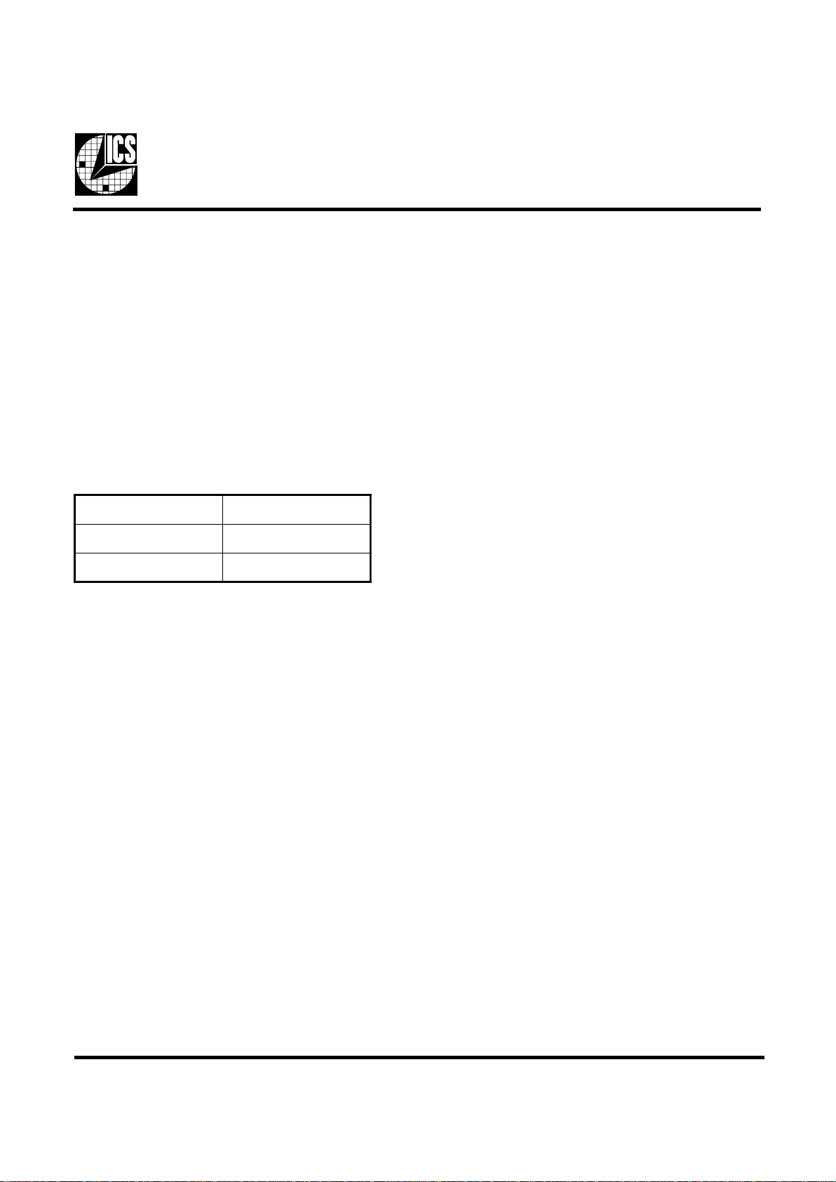
Mode Pin - Power Management Input Control
EDOM
)tupnIdehctaL(
0
#POTS_ICP
)tupnI(
1
0FER
)tuptuO(
4
ICS92 50-08
Third party brands and names are the property of their respective owners.
1. The ICS clock generator is a slave/receiver, I2C component. It can read back the data stored in the latches for
verification. Read-Back will support Intel PIIX4 "Block-Read" protocol.
2. The data transfer rate supported by this clock generator is 100K bits/sec or less (standard mode)
3. The input is operating at 3.3V logic levels.
4. The data byte format is 8 bit bytes.
5. To simplify the clock generator I
2
C interface, the protocol is set to use only "Block-Writes" from the controller. The
bytes must be accessed in sequential order from lowest to highest byte with the ability to stop after any complete byte
has been transferred. The Command code and Byte count shown above must be sent, but the data is ignored for those
two bytes. The data is loaded until a Stop sequence is issued.
6. At power-on, all registers are set to a default condition, as shown.
General I2C serial interface information
The information in this section assumes familiarity with I2C programming.
For more information, contact ICS for an I
2
C programming application note.
How to Write:
Controller (host) sends a start bit.
Controller (host) sends the write address D2
(H)
ICS clock will acknowledge
Controller (host) sends a dummy command code
ICS clock will acknowledge
Controller (host) sends a dummy byte count
ICS clock will acknowledge
Controller (host) starts sending first byte (Byte 0)
through byte 5
ICS clock will acknowledge each byte one at a time.
Controller (host) sends a Stop bit
How to Read:
Controller (host) will send start bit.
Controller (host) sends the read address D3
(H)
ICS clock will acknowledge
ICS clock will send the byte count
Controller (host) acknowledges
ICS clock sends first byte (Byte 0) through byte 5
Controller (host) will need to acknowledge each byte
Controller (host) will send a stop bit
Notes:
Controller (Host) ICS (Slave/Receiver)
Start Bit
Address
D3
(H)
AC
K
Byte Count
ACK
Byte
0
ACK
Byte 1
ACK
Byte
2
ACK
Byte
3
ACK
Byte 4
ACK
Byte
5
ACK
Stop Bit
How to Read:
Controller (Host) ICS (Slave/Receiver)
Start Bit
Address
D2
(H)
AC
K
Dummy Command Code
AC
K
Dummy Byte Count
AC
K
Byte 0
AC
K
Byte 1
ACK
Byte 2
AC
K
Byte 3
AC
K
Byte 4
AC
K
Byte 5
AC
K
Stop Bit
How to Write:
5
ICS92 50-08
Third party brands and names are the property of their respective owners.
tiBnoitpircseDDWP
7tiB
noitaludoMmurtcepSdaerpS%52.0±-0
noitaludoMmurtcepSdaerpS%5.0±-1
0
4tiB5tiB6tiB2tiBkcolcUPCICP
1etoN
,2tiB
4:6tiB
1110
0110
3.001
331
)3/UPC(34.33
)3/UPC(33.44
1010
0010
211
301
)3/UPC(33.73
)3/UPC(3.43
1100
0100
8.66
3.38
)2/UPC(4.33
)2/UPC(56.14
1000
0000
57
421
)2/UPC(5.73
)3/UPC(33.14
1111
0111
331
421
)4/UPC(52.33
)4/UPC(00.13
1011
0011
051
041
)4/UPC(05.73
)4/UPC(00.53
1101
0101
501
011
)3/UPC(00.53
)3/UPC(76.63
1001
0001
511
021
)3/UPC(33.83
)3/UPC(00.04
3tiB
stupnIdehctaL,tceleserawdrahybdetcelessiycneuqerF-0
)evoba(4:6,2tiBybdetcelessiycneuqerF-1
0
1tiB
lamroN-0
)daerpSretneC(delbanEmurtcepSdaerpS-1
0
0tiB
gninnuR-0
stuptuollaetatsirT-1
0
Byte0: Functionality and Frequency Select Register (default = 0)
Serial Configuration Command Bitmap
Note: PWD = Power-Up Default
Note 1. Default at Power-up will be for latched logic inputs to define frequency. Bits 2, 4, 5,
6 are default to 0000, and if bit 3 is written to a 1 to use Bits 2, 6:4, then these
should be defined to desired frequency at same write cycle.

6
ICS92 50-08
Third party brands and names are the property of their respective owners.
Byte 1: CPU, Active/Inactive Register
(1= enable, 0 = disable)
TIB#NIPDWPNOITPIRCSED
7tiB-1 devreseR
6tiB-1 devreseR
5tiB-1 devreseR
4tiB-1 devreseR
3tiB641 )tcanI/tcA(F_MARDS
2tiB941 )tcanI/tcA(2KLCUPC
1tiB151 )tcanI/tcA(1KLCUPC
0tiB251 )tcanI/tcA(F_KLCUPC
Byte 2: PCI, Active/Inactive Register
(1= enable, 0 = disable)
TIB#NIPDWPNOITPIRCSED
7tiB-1 devreseR
6tiB81 )tcanI/tcA(F_KLCICP
5tiB611 )tcanI/tcA(5KLCICP
4tiB411 )tcanI/tcA(4KLCICP
3tiB311 )tcanI/tcA(3KLCICP
2tiB211 )tcanI/tcA(2KLCICP
1tiB111 )tcanI/tcA(1KLCICP
0tiB91 )tcanI/tcA(0KLCICP
Notes:
1. Inactive means outputs are held LOW and are disabled
from switching.
2. Latched Frequency Selects (FS#) will be inferted logic
load of the input frequency select pin conditions.
TIB#NIPDWPNOITPIRCSED
7tiB-X #0SFdehctaL
6tiB-1 devreseR
5tiB-1 devreseR
4tiB-X #1SFdehctaL
3tiB-1 devreseR
2tiB-1 devreseR
1tiB-X #3SFdehctaL
0tiB-1 devreseR
Byte 4: Reserved , Active/Inactive Register
(1= enable, 0 = disable)
TIB#NIPDWPNOITPIRCSED
7tiB-1 devreseR
6tiB-X #2SFdehctaL
5tiB451 )tcanI/tcA(F_CIPAOI
4tiB551 )tcanI/tcA(0CIPAOI
3tiB-1 devreseR
2tiB-1 devreseR
1tiB21 )tcanI/tcA(1FER
0tiB31 )tcanI/tcA(0FER
Byte 5: Peripheral , Active/Inactive Register
(1= enable, 0 = disable)
Byte 3: SDRAM, Active/Inactive Register
(1= enable, 0 = disable)
TIB#NIPDWPNOITPIRCSED
7tiB-1 devreseR
6tiB-1 devreseR
5tiB031 )tcanI/tcA(zHM42
4tiB921 )tcanI/tcA(zHM84
3tiB
,23,33
42,52
1)tcanI/tcA()51:21(MARDS
2tiB
,12,22
81,91
1)tcanI/tcA()11:8(MARDS
1tiB
,83,93
53,63
1)tcanI/tcA()7:4(MARDS
0tiB
,34,44
04,14
1)tcanI/tcA()3:0(0MARDS

7
ICS92 50-08
Third party brands and names are the property of their respective owners.
Shared Pin Operation Input/Output Pins
Fig. 1
The I/O pins designated by (input/output) on the ICS925008 serve as dual signal functions to the device. During initial
power-up, they act as input pins. The logic level (voltage)
that is present on these pins at this time is read and stored
into a 4-bit internal data latch. At the end of Power-On reset,
(see AC characteristics for timing values), the device changes
the mode of operations for these pins to an output function.
In this mode the pins produce the specified buffered clocks
to external loads.
To program (load) the internal configuration register for these
pins, a resistor is connected to either the VDD (logic 1)
power supply or the GND (logic 0) voltage potential. A 10
Kilohm(10K) resistor is used to provide both the solid CMOS
programming voltage needed during the power-up
programming period and to provide an insignificant load on
the output clock during the subsequent operating period.
Figs. 1 and 2 show the recommended means of implementing
this function. In Fig. 1 either one of the resistors is loaded
onto the board (selective stuffing) to configure the devices
internal logic. Figs. 2a and b provide a single resistor loading
option where either solder spot tabs or a physical jumper
header may be used.
These figures illustrate the optimal PCB physical layout
options. These configuration resistors are of such a large
ohmic value that they do not effect the low impedance clock
signals. The layouts have been optimized to provide as little
impedance transition to the clock signal as possible, as it
passes through the programming resistor pad(s).

8
ICS92 50-08
Third party brands and names are the property of their respective owners.
Fig. 2a
Fig. 2b

9
ICS92 50-08
Third party brands and names are the property of their respective owners.
CPU_STOP# Timing Diagram
CPUSTOP# is an asychronous input to the clock synthesizer. It is used to turn off the CPUCLKs for low power operation.
CPU_STOP# is synchronized by the ICS9250-08. All other clocks will continue to run while the CPUCLKs are disabled. The
CPUCLKs will always be stopped in a low state and start in such a manner that guarantees the high pulse width is a full pulse.
CPUCLK on latency is less than 4 CPUCLKs and CPUCLK off latency is less than 4 CPUCLKs.
Notes:
1. All timing is referenced to the internal CPUCLK.
2. CPU_STOP# is an asynchronous input and metastable conditions may exist. This signal is synchronized to the
CPUCLKs inside the ICS9250-08.
3. IOAPIC output is stopped Glitch Free by CPUSTOP# going low.
4. PCI_STOP# is shown in a high (true) state.
5. All other clocks continue to run undisturbed.
Notes:
1. All timing is referenced to the Internal CPUCLK (defined as inside the device.)
2. PCI_STOP# is an asynchronous input, and metastable conditions may exist. This signal is required to be synchronized
inside the device.
3. All other clocks continue to run undisturbed.
4. CPU_STOP# is shown in a high (true) state.
PCI_STOP# Timing Diagram
PCI_STOP# is an asynchronous input to the ICS9250-08. It is used to turn off the PCICLK (0:5) clocks for low power operation.
PCI_STOP# is synchronized by the ICS9250-08 internally. PCICLK (0:5) clocks are stopped in a low state and started with a full
high pulse width guaranteed. PCICLK (0:5) clock on latency cycles are only one rising PCICLK clock off latency is one PCICLK
clock.

10
ICS92 50-08
Third party brands and names are the property of their respective owners.
Absolute Maximum Ratings
Supply Voltage . . . . . . . . . . . . . . . . . . . . . . . . . . . . 7.0 V
Logic Inputs . . . . . . . . . . . . . . . . . . . . . . . . . . . . . . GND 0.5 V to V
DD
+0.5 V
Ambient Operating Temperature . . . . . . . . . . . . . 0°C to +70°C
Case Temperature . . . . . . . . . . . . . . . . . . . . . . . . . . 115°C
Storage Temperature . . . . . . . . . . . . . . . . . . . . . . . 65°C to +150°C
Stresses above those listed under Absolute Maximum Ratings may cause permanent damage to the device. These ratings are
stress specifications only and functional operation of the device at these or any other conditions above those listed in the
operational sections of the specifications is not implied. Exposure to absolute maximum rating conditions for extended periods
may affect product reliability.
Electrical Characteristics - Input/Supply/Common Output Parameters
TA = 0 - 70º C; Supply Voltage VDD = 3.3 V +/-5%, V
DDL
= 2.5 V +/-5% (unless otherwise stated)
PARAMETER SYMBOL CONDITIONS MIN TYP MAX UNITS
Operating
I
DD2.5OP66
Select @ 66MHz; Max discrete cap loads
10
25
Operating I
DD2.5OP100
Select @ 100MHz; Max discrete cap loads
13
25
Supply Current
I
DD2.5OP133
Select @ 133MHz; Max discrete cap loads
18
25
1
Guaranteed by design, not 100% tested in production.
mA
Electrical Characteristics - Input/ Supply/Common Output Parameters
TA = 0 - 70º C; Supply Voltage VDD = 3.3 V +/-5%, V
DDL
= 2.5 V +/-5% (unless otherwise stated)
PARAMETER SYMBOL CONDITIONS MIN TYP MAX UNITS
Input High Voltage V
IH
2V
DD
+0.3 V
Input Low Voltage V
IL
VSS-0.3 0.8 V
Input High Current I
IH
VIN = V
DD
0.1 5
µ
A
Input Low Current I
IL1
VIN = 0 V; Inputs with no pull-up resistors -5 2.0
µ
A
Input Low Current I
IL2
VIN = 0 V; Inputs with pull-up resistors -200 -100
µ
A
I
DD3.3OP66
Select @ 66MHz; Sdram running, unloaded 112 140
I
DD3.3OP100
Select @ 100MHz; Sdram running, unloaded 150
180
I
DD3.3OP133
Select @ 133MHz; Sdram running, unloaded 200
250
Input frequency F
i
VDD = 3.3 V 12 14. 318 16 MHz
C
IN
Logic Inputs 5 pF
C
INX
X1 & X2 pins 27 36 45 pF
Transition Time
1
T
Trans
To 1st crossing of target Freq. 3 ms
Settling Time
1
T
S
From 1st crossing to 1% target Freq. 1 3 ms
Clk Stabilization
1
T
Stab
From VDD = 3.3 V to 1% target Freq.
3ms
1
Guaranteed by design, not 100% tested in produc tion.
mA
Operating Supply
Current
Input Capacitance
1

11
ICS92 50-08
Third party brands and names are the property of their respective owners.
Electrical Characteristics - CPUCLK
TA = 0 - 70º C; VDD = 3.3 V +/-5%, V
DDL
= 2.5 V +/-5%; CL = 20 pF (unless otherwise stated)
PARAMETER SYMBOL CONDITIONS MIN TYP MAX UNITS
Output High Voltage V
OH2B
IOH = -12.0 mA 2 2.3 V
Output Low Voltage V
OL2B
IOL = 12 mA 0.3 0.4 V
Output High Current I
OH2B
VOH = 1.7 V -35 -19 mA
Output Low Current I
OL2B
VOL = 0.7 V 19 26 mA
Rise Time t
r2B
1
VOL = 0.4 V, VOH = 2.0 V 0.4 1.4 1.8 ns
Fall Time t
f2B
1
VOH = 2.0 V, VOL = 0.4 V 0.4 1.35 1.8 ns
d
t1B
1
VT = 1.25 V; CPU < 120MHz 45 45 55
d
t2B
1
VT = 1.25 V; CPU >= 124MHz 35 43 50
t
sk2B
1
VT = 1.25 V; CPU >= 100 MHz 150 175
t
sk2B
1
VT = 1.25 V; CPU < 100 MHz 170 240
Jitter, One Sigma t
j
1σ2B
1
VT = 1.25 V 35 150
Jitter, Absolute t
j
abs2B
1
VT = 1.25 V -250 99 +250
Jitter, Cycle-to-cycle
t
jcyc-cyc2B
1
VT = 1.25 V
210 250
1
Guaranteed by design, not 100% tested in production.
ps
%Duty Cycle
Skew ps
Electrical Characteristics - PCICLK
TA = 0 - 70º C; VDD = 3.3 V +/-5%, V
DDL
= 2.5 V +/-5%; CL = 60 pF for PCI0 & PCI1, CL = 30 pF for other PCIs
PARAMETER SYMBOL CONDITIONS MIN TYP MAX UNITS
Output High Voltage V
OH1
IOH = -18 mA 2.4 2.9 V
Output Low Voltage V
OL1
IOL = 9.4 mA 0.2 0.4 V
Output High Current I
OH1
VOH = 2.0 V -52 -22 mA
Output Low Curr e nt I
OL1
VOL = 0.8 V 25 41 mA
Rise Time
1
t
r1
VOL = 0.4 V, VOH = 2.4 V 0.5 2.2 2.6 ns
Fall Time
1
t
f1
VOH = 2.4 V, VOL = 0.4 V 0.5 1.8 2.2 ns
Duty Cycle
1
d
t1
VT = 1.5 V 46 50 56 %
t
sk1
VT = 1.5 V; All PCI clocks including PCI0 400 850
t
sk1
VT = 1.5 V; All PCI clocks except PCI0 250 500
Jitter, One Sigma
1
t
j
1σ1
VT = 1.5 V 15 150
Jitter, Absolute
1
t
j
abs1
VT = 1.5 V -250 60 250
1
Guaranteed by design, not 100% tested in production.
ps
Skew
1
window
ps

12
ICS92 50-08
Third party brands and names are the property of their respective owners.
Electrical Characteristics - SDRAM
TA = 0 - 70º C; VDD = 3.3 V +/-5%, V
DDL
= 2.5 V +/-5%; CL =30 pF
PA RAMETER SYMBOL CONDITIONS MIN TYP MAX UNITS
Output High Voltage V
OH1
IOH = -28 mA 2.4 2.8 V
Output Low Voltage V
OL1
IOL = 19 mA 0.34 0.4 V
Output High Current I
OH1
VOH = 2.0 V -100 -42 mA
Output Low C urrent I
OL1
VOL = 0.8 V 33 42 mA
t
r1
VOL = 0.4 V, VOH = 2.4 V; 66, 75, 83 MHz 0.5 1.6 2.2
t
r1
VOL = 0.4 V, VOH = 2.4 V; >= 100 MHz 0.5 1.3 1.6
t
f1
VOH = 2.4 V, VOL = 0.4 V; 66, 75, 83 MHz 0.5 1.5 2.3
t
f1
VOH = 2.4 V, VOL = 0.4 V; >= 100 MHz 0.5 1.5 1.8
Duty Cycle
1
d
t1
VT = 1.5 V; Input Duty Cycle at 50% 47 52 57 %
t
sk1
VT = 1.5 V; SD_F to 0:6, 8:10 150 250
t
sk1
VT = 1.5 VSD_F to 7, 12:15 210 400
Jitter, One Sigma
1
t
j1σ1
VT = 1.5 V 50 150
Jitter, Absolute
1
t
jabs1
VT = 1.5 V -250 130 250
1
Guaranteed by design, not 100% tested in production.
Skew
1
Window
ps
Rise Time
1
Fall Time
1
ns
Electrical Characteristics - IOAPIC
TA = 0 - 70º C; VDD = 3.3 V +/-5%, V
DDL
= 2.5 V +/-5%; CL = 20 pF (unless otherwise st ated)
PARAMETER SYMBOL CONDITIONS MIN TYP MAX UNITS
Output High Volt age V
OH4B
IOH = -8 mA 2 2.2 V
Output Low Voltage V
OL4B
IOL = 12 mA 0.3 0.4 V
Output High Current I
OH4B
VOH = 1.7 V -24 -15 mA
Output Low Current I
OL4B
VOL = 0.7 V 19 26 mA
Rise Time
1
T
r4B
VOL = 0.4 V, VOH = 2.0 V 0.4 1.3 1.6 ns
Fall Time
1
T
f4B
VOH = 2.0 V, VOL = 0.4 V 0.4 2 2.6 ns
Duty Cycle
1
D
t4B
VT = 1.25 V 45 51 55 %
Jitter, One Sigma
1
T
j
1σ4B
VT = 1.25 V 240 300 ps
Jitter, Absolute
1
T
jabs4B
VT = 1.25 V
625 650 ps
1
Guaranteed by design, not 100% tested in production.

13
ICS92 50-08
Third party brands and names are the property of their respective owners.
Electrical Characteristics - 48MHz, 24MHz,REF0
TA = 0 - 70º C; VDD = 3.3 V +/-5%, V
DDL
= 2.5 V +/-5%; CL = 20 pF (unless otherwise stated)
PA RAMETER S YMBOL CONDITIONS M IN TYP M AX UNIT S
Output High Voltage V
OH5
IOH = -12 mA 2.4 2.8 V
Output L ow Voltage V
OL5
IOL = 12 mA 0.2 0.4 V
Output High Current I
OH5
VOH = 2.0 V -33 -20 mA
Output L ow Current I
OL5
VOL = 0.8 V 10 32 mA
Rise Time
1
t
r5
VOL = 0.4 V, VOH = 2.4 V, 48MHz 2 4 ns
Fall Time
1
t
f5
VOH = 2.4 V, VOL = 0.4 V, 48MHz 1.8 4 ns
Duty Cycle
1
d
t5
VT = 1.5 V, 48MHz 45 50 55 %
Rise Time
1
t
r5
VOL = 0.4 V, VOH = 2.4 V, REF0 2.2 4 ns
Fall Time
1
t
f5
VOH = 2.4 V, VOL = 0.4 V, REF0 1.8 4 ns
Duty Cycle
1
d
t5
V T = 1.5 V, REF 45 52 55 %
Jitter, Cycle-to-cycle
1
t
jcy
c-cyc5
VT = 1.5 V, 24, 48MHz 700 1100 ps
Jitter, Cycle-to-cycle
1
t
jcyc-cyc5
VT = 1.5 V, REF0
500 800 ps
1
Guaranteed by design, not 100% tested in production.
Electrical Characteristics - REF1
TA = 0 - 70º C; VDD = 3.3 V +/-5%, V
DDL
= 2.5 V +/-5%; CL = 20 pF (unless otherwise stated)
PARAMETER SYMBOL CONDITIONS MIN TYP MAX UNITS
Output High Voltage V
OH5
IOH = -14 mA 2.4 2.8 V
Output Low Voltage V
OL5
IOL = 6 mA 0.2 0.4 V
Output High Current I
OH5
VOH = 2.0 V -28 -20 mA
Output Low Current I
OL5
VOL = 0.8 V 10 22 mA
Rise Time
1
t
r5
VOL = 0.4 V, VOH = 2.4 V, REF1 2.5 4 ns
Fall Time
1
t
f5
VOH = 2.4 V, VOL = 0.4 V, REF1 2.2 4 ns
Duty Cycle
1
d
t5
VT = 1.5 V, REF1 45 50 55 %
Jitter, Cycle-to-cycle
1
t
jcyc-cyc5
VT = 1.5 V, REF1
600 800 ps
1
Guaranteed by design, not 100% tested in production.

14
ICS92 50-08
Third party brands and names are the property of their respective owners.
General Layout Precautions:
1) Use a ground plane on the top layer
of the PCB in all areas not used by
traces.
2) Make all power traces and ground
traces as wide as the via pad for lower
inductance.
Notes:
1) All clock outputs should have a
series terminating resistor, and a 20pF
capacitor to ground between the
resistor and clock pin. Not shown in
all places to improve readibility of
diagram.
2) Optional crystal load capacitors are
recommended. They should be
included in the layout but not
inserted unless needed.
Component Values:
C1 : Crystal load values determined by user
C2 : 22µF/20V/D case/Tantalum
AVX TAJD226M020R
C3 : 100pF ceramic capacitor
C4 : 20pF capacitor
FB = Fair-Rite products 2512066017X1
All unmarked capacitors are 0.01µF ceramic
Connections to VDD:
= Routed Power
= Ground Connection (component side copper)
= Ground Plane Connection
= Power Route Connection
= Solder Pads
= Clock Load
Ferrite
Bead
VDD
C2
22µF/20V
Tantalum
Ferrite
Bead
VDD
C2
22µF/20V
Tantalum
C3
C3
1
Clock Load
56
55
54
53
52
51
50
49
48
47
46
45
44
43
42
41
40
39
38
37
36
35
34
33
32
31
30
29
2
C1
C1
1
2
3
4
5
6
7
8
9
10
11
12
13
14
15
16
17
18
19
20
21
22
23
24
25
26
27
28
3.3V Power Route
3.3V Power Route
Ground
Ground
2.5V Power Route

15
ICS92 50-08
Third party brands and names are the property of their respective owners.
LOBMYS SNOISNEMIDNOMMOC SNOITAIRAV D N
.NIM.MON.XAM.NIM.MON.XAM
A590.101.011.DA027.527.037.65
1A800.210.610.
2A880.090.290.
B800.010.5310.
C500.- 010.
DsnoitairaVeeS
E292.692.992.
eCSB520.0
H004.604.014.
h010.310.610.
L420.230.040.
NsnoitairaVeeS
µ
°0 °5 °8
X580.390.001.
SSOP Package
Ordering Information
ICS9250yF-08
Pattern Number (2 or 3 digit number for parts with ROM code patterns)
Package Type
F=SSOP
Revision Designator (will not correlate with datasheet revision)
Device Type (consists of 3 or 4 digit numbers)
Prefix
ICS, AV = Standard Device
Example:
ICS XXXX y F - PPP
ICS reserves the right to make changes in the device data identified in
this publication without further notice. ICS advises its customers to
obtain the latest version of all device data to verify that any
information being relied upon by the customer is current and accurate.
 Loading...