

ICST AV9248F-107, ICS9248F-107 Datasheet
Integrated
Circuit
Systems, Inc.
ICS9248-107
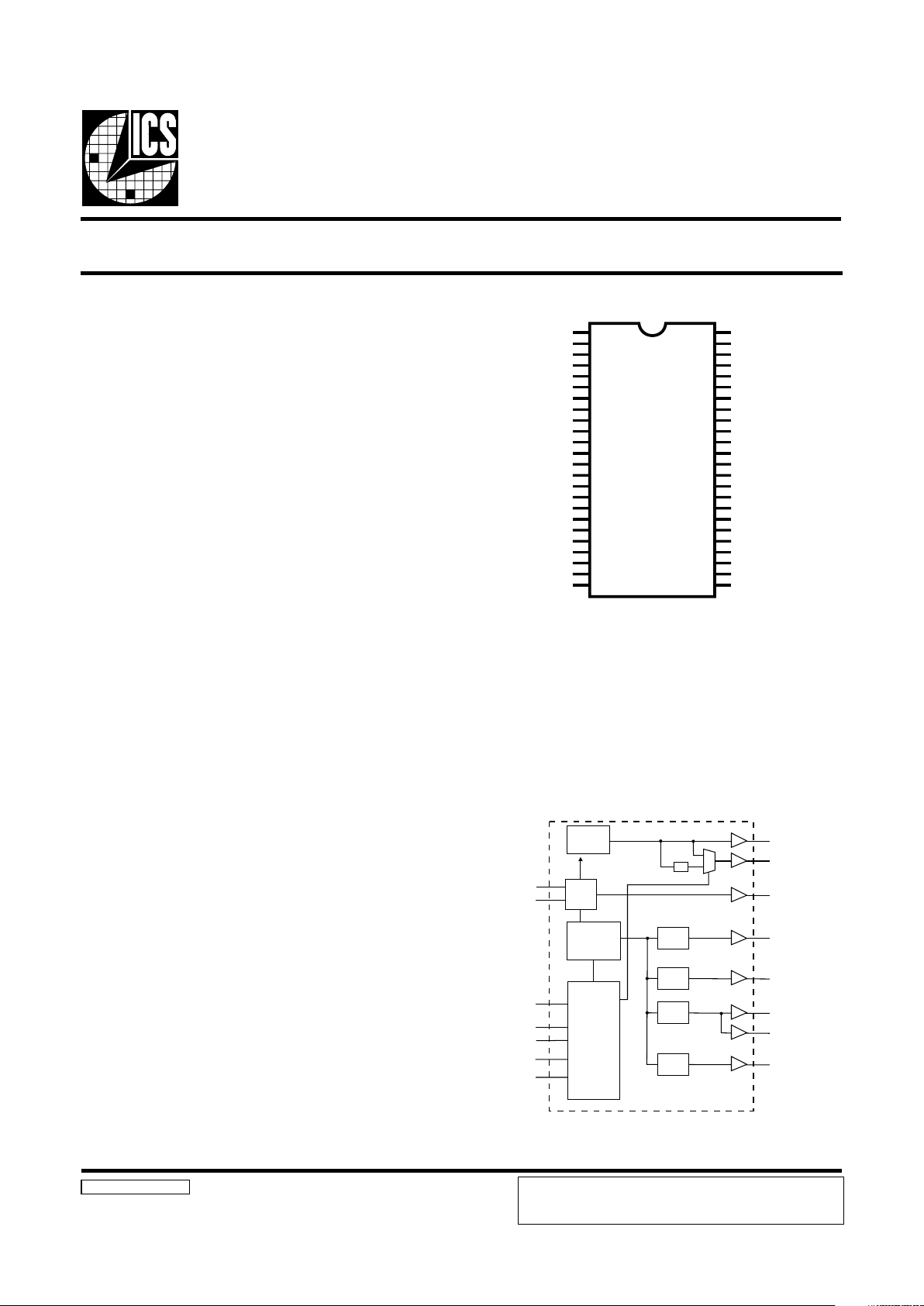
Block Diagram
Frequency Timing Generator for PENTIUM II Systems
9248-107 RevA - 5/21/01
Pin Configuration
48-pin SSOP
*120K ohm pull-up to VDD on indicated inputs.
Recommended Application:
RCC chipset
Output Features:
• 4 - CPUs @ 2.5V , up to 180MHz.
• 3 - IOAPIC @ 2.5V
• 3 - 3V66MHz @ 3.3V .
• 11 - PCIs @ 3.3V
• 1 - 48MHz, @ 3.3V fixed
• 1 - 24/48MHz, @ 3.3V
Features:
• Up to 180MHz frequency support
• Use a zero delay buffer such as the ICS9179-06 to
generate SDRAM clocks.
• Support power management: Power down Mode
from I2C programming.
• Spread spectrum for EMI control
± 0.25% center spread).
• Uses external 14.318MHz crystal
• 5 - FS pins for frequency select
Key Specifications:
• CPU Output Jitter: <250ps
• IOAPIC Output Jitter: <500ps
• 48MHz, 3V66, PCI Output Jitter: <500ps
• Ref Output Jitter. <1000ps
• CPU Output Skew: <175ps
• IOAPIC Output Skew <250ps
• PCI Output Skew: <580ps
• 3V66 Output Skew <250ps
• CPU to 3V66 Output Offset: 0.8 - 1.8ns (typ = 1.3ns)
• CPU to PCI Output Offset: 0.0 - 1.5ns (typ = 1.0ns)
• CPU to IOAPIC Output Offset: 1.5 - 4.0ns (typ = 2.0ns)
SEL24_48#
PLL2
PLL1
Spread
Spectrum
48MHz
24_48MHz
CPUCLK (3:0)
IOAPIC (2:0)
PCICLK (10:0)
PCICLK_F
3V66 (2:0)
X1
X2
XTAL
OSC
CPU
DIVDER
IOAPIC
DIVDER
PCI
DIVDER
3V66
DIVDER
S DATA
SCLK
IC
2
FS(4:0)
PD#
Control
Logic
Config.
Reg.
/ 2
REF(1:0)
{
GNDREF
REF0
*SEL24_48#/REF1
VDDREF
X1
X2
GNDPCI
*FS0/PCICLK_F
*FS1/PCICLK1
VDDPCI
*FS2/PCICLK2
*FS3/PCICLK3
GNDPCI
PCICLK4
PCICLK5
VDDPCI
PCICLK6
PCICLK7
GNDPCI
PCICLK8
PCICLK9
PCICLK10
VDDPCI
PD#
ICS9248-107
1
2
3
4
5
6
7
8
9
10
11
12
13
14
15
16
17
18
19
20
21
22
23
24
48
47
46
45
44
43
42
41
40
39
38
37
36
35
34
33
32
31
30
29
28
27
26
25
VDDLAPIC
IOAPIC0
IOAPIC1
GNDLAPIC
IOAPIC2
VDDLCPU
CPUCLK0
GNDLCPU
CPUCLK1
VDDLCPU
CPUCLK2
CPUCLK3
GNDLCPU
VDD66
3V66_0
3V66_1
3V66_2
GND66
S DATA
SCLK
VDD48
48MHz/FS4*
24_48MHz
GND48
{
I
C
2
ICS reserves the right to make changes in the device data identified in
this publication without further notice. ICS advises its customers to
obtain the latest version of all device data to verify that any
information being relied upon by the customer is current and accurate.
2
ICS9248-107
Pin Descriptions
The ICS9248-107 is a main clock synthesizer chip for Pentium II based systems using Rambus Interface DRAMs. This chip
provides all the clocks required for such a system when used with a zero delay buffer such as the ICS9179-06.
Spread Spectrum may be enabled through I2C. Spread spectrum typically reduces system EMI by 8dB to 10dB. This simplifies
EMI qualification without resorting to board design iterations or costly shielding. The ICS9248-107 employs a proprietary
closed loop design, which tightly controls the percentage of spreading over process and temperature variations.
General Description
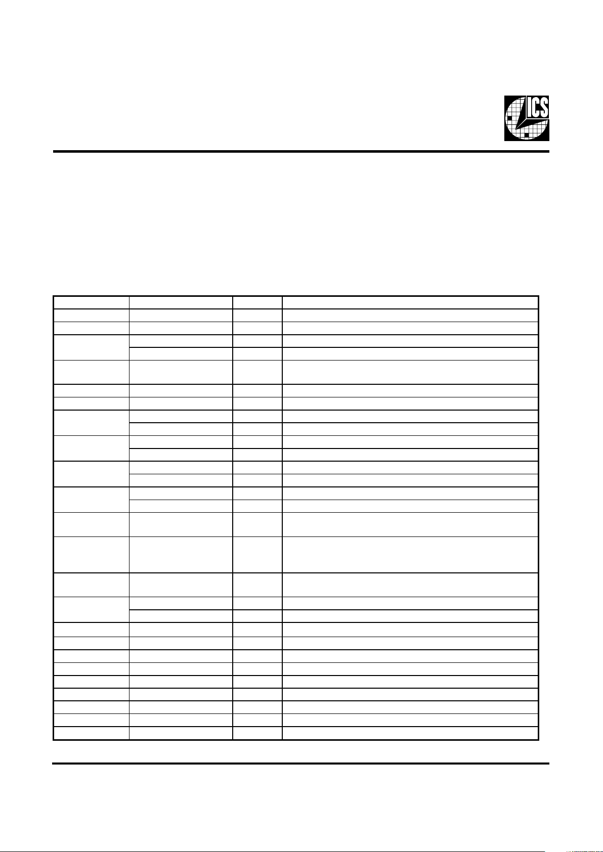
Pin number Pin name Type Description
1, 7, 13, 19, 25, 31 GND PWR Ground pins
2 REF0 OUT 14.318MHz reference clock outputs at 3.3V
REF1 OUT 14.318MHz reference clock outputs at 3.3V
SEL24_48# IN Logic input to select 24 or 48MHz for pin 26 output
4, 10, 16, 23,
28, 35
VDD PWR Power pins 3.3V
5 X1 IN X TAL_IN 14.318M Hz crystal input
6 X 2 OU T XTAL_OUT Crystal output
PCICLK_F OUT Free running PCI clock at 3.3V. Synchronous to CPU clocks.
FS 0 IN Logic - input for frequency selection
PCICLK1 OUT PCI clock output at 3.3V. Synchronous to CPU clocks.
FS 1 IN Logic - input for frequency selection
PCICLK2 OUT PCI clock output at 3.3V. Synchronous to CPU clocks.
FS 2 IN Logic - input for frequency selection
PCICLK3 OUT PCI clock output at 3.3V. Synchronous to CPU clocks.
FS 3 IN Logic - input for frequency selection
14, 15, 17, 18, 20,
21, 22
PCICLK (4:10) OUT PCI clock outputs at 3.3V. Synchronous to CPU clocks.
24 PD# IN
This asynchronous input powers down the chip when drive
active(Low). The internal PLLs are dis abled and all the output clocks
are held at a Low s tate.
26 24_48MHz OUT
24 or 48MHz output selectable by
SEL24_48# (0=48MHz 1=24MHz)
48MHz OUT Fixed 48MHz clock output at 3.3V
FS 4 IN Logic - input for frequency selection
29 SCLK IN
Clock in
p
ut of I2C input
30 SDATA I/O Data pin for I2C circuitry 5V tolerant
32, 33, 34 3V66(2:0) OUT 3.3V clock outputs.
36, 41 GNDLCPU PWR Ground pins for CPUCLKs
37, 38, 40, 42 CPUCLK(3:0) OUT Host bus clock output at 2.5V.
39, 43 VDDLCPU PWR Power pins for CPUCLKs. 2.5V
45 GNDLAPIC PWR Ground pin for the IOAPIC outputs.
44, 46, 47 IOAPIC(2:0) OUT IOAPIC clocks at 2.5V. Synchronous with CPUCLKs.
48 VDDLAPIC PWR Power pin for the IOAPIC outputs. 2.5V.
27
12
3
8
9
11
3
ICS9248-107
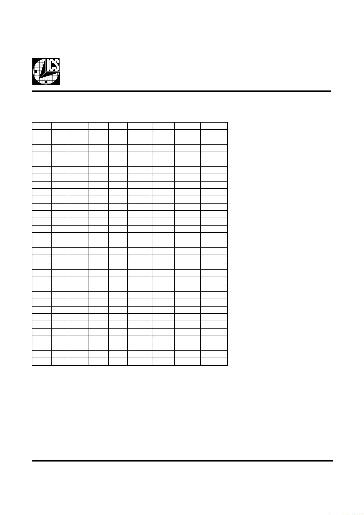
Functionality
FS4 FS3 FS2 FS1 FS0 CPU PCI 3V66 IOAPI C
0 0 0 0 0 103.0 34.33 68.67 17.17
0 0 0 0 1 100.0 33.33 66.67 16.67
0 0 0 1 0 100.5 33.48 66.97 16.74
0 0 0 1 1 100.9 33.63 67.27 16.82
0 0 1 0 0 107.1 35.70 71.40 17.85
0 0 1 0 1 109.0 36.33 72.67 18.17
0 0 1 1 0 112.0 37.33 74.67 18.67
0 0 1 1 1 114.0 28.50 57.00 14.25
0 1 0 0 0 116.0 29.00 58.00 14.50
0 1 0 0 1 118.0 29.50 59.00 14.75
0 1 0 1 0 133.3 33.33 66.65 16.66
0 1 0 1 1 120.0 30.00 60.00 15.00
0 1 1 0 0 122.0 30.50 61.00 15.25
0 1 1 0 1 125.0 31.25 62.50 15.63
0 1 1 1 0 50.0 16.67 33.33 8.33
0 1 1 1 1 66.7 16.67 33.33 8.33
1 0 0 0 0 133.3 33.33 66.67 16.67
1 0 0 0 1 133.9 33.48 66.95 16.74
1 0 0 1 0 138 34.5 69 17.25
1 0 0 1 1 142 35.5 71 17.75
1 0 1 0 0 146 36.5 73 18.25
1 0 1 0 1 150 37.5 75 18.75
1 0 1 1 0 153 38.25 76.5 19.13
1 0 1 1 1 156 39 78 19.5
1 1 0 0 0 159.1 39.78 79.55 19.89
1 1 0 0 1 162 40.5 81 20.25
1 1 0 1 0 166.7 41.67 83.33 20.83
1 1 0 1 1 168 42 84 21
1 1 1 0 0 171 42.75 85.5 21.38
1 1 1 0 1 174 43.5 87 21.75
1 1 1 1 0 177 44.25 88.5 22.13
1 1 1 1 1 180 45 90 22.5
4
ICS9248-107
Byte 0: Functionality and frequency select register (Default = 0)
Serial Configuration Command Bitmap
Note 1:
Default at power-up will be for latched logic inputs to define frequency , as displayed byBit 3.
tiBnoitpircseDDWP
tiB
)4:7,2(
2tiB
4SF
7tiB
3SF
6tiB
2SF
5tiB
1SF
4tiB
0SF
UPCICP66V3CIPAOI
01000
1etoN
00000 0.30133.4376.8671.71
00001 0.00133.3376.6676.61
00010 54.00184.3379.6647.61
00011 9.00136.3372.7628.61
00100 1.70107.5304.1758.71
00101 0.90133.6376.2771.81
00110 0.21133.7376.4776.81
00111 00.41105.8200.7552.41
01000 00.61100.9200.8505.41
01001 00.81105.9200.9557.41
01010 03.33133.3356.6666.61
01011 00.02100.0300.0600.51
01100 00.22105.0300.1652.51
01101 00.52152.1305.2636.51
01110 0.0576.6133.3333.8
01111 7.6676.6133.3333.8
10000 3.33133.3376.6676.61
10001 9.33184.3359.6647.61
10010 0.83105.4300.9652.71
10011 0.24105.5300.1757.71
10100 0.64105.6300.3752.81
10101 0.05105.7300.5757.81
10110 0.35152.8305.6731.91
10111 0.65100.9300.8705.91
11000 1.95187.9355.9798.91
11001 0.26105.0400.1852.02
11010 7.66176.1433.3838.02
11011 0.86100.2400.4800.12
11100 0.17157.2405.5883.12
11101 0.47105.3400.7857.12
11110 0.77152.4405.8831.22
11111 0.08100.5400.0905.22
3tiB
stupnidehctal,tceleserawdrahybdetcelessiycneuqerF-0
4:7,2tiBybdetcelessiycneuqerF-1
0
1tiB
lamroN-0
delbanemurtcepsdaerpS-1
1
0tiB
gninnuR-0
stuptuollaetatsirT-1
0
5
ICS9248-107
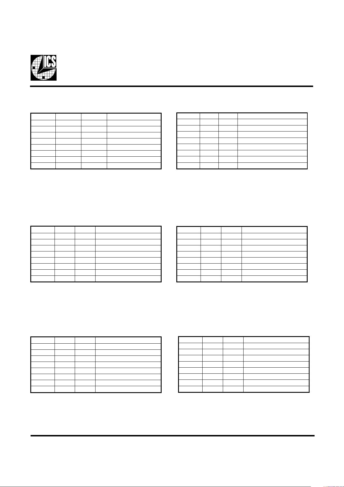
Byte 1: CPU, Active/Inactive Register
(1 = enable, 0 = disable)
Byte 2: PCI Active/Inactive Register
(1 = enable, 0 = disable)
Byte 3: 3V66 Active/Inactive Register
(1 = enable, 0 = disable)
Notes:
1. Inactive means outputs are held LOW and are disabled
from switching.
Notes:
1. Inactive means outputs are held LOW and are disabled
from switching.
Notes:
1. Inactive means outputs are held LOW and are disabled
from switching.
Byte 4: PCI Active/Inactive Register
(1 = enable, 0 = disable)
Notes:
1. Inactive means outputs are held LOW and are disabled
from switching.
tiB#niPDWPnoitpircseD
7tiB041 1KLCUPC
6tiB831 2KLCUPC
5tiB731 3KLCUPC
4tiB241 0KLCUPC
3tiB741 0CIPAOI
2tiB641 1CIPAOI
1tiB441 2CIPAOI
0tiB-X )devreseR(
tiB#niPDWPnoitpircseD
7tiB811 7KLCICP
6tiB711 6KLCICP
5tiB511 5KLCICP
4tiB411 4KLCICP
3tiB211 3KLCICP
2tiB111 2KLCICP
1tiB91 1KLCICP
0tiB81 F_KLCICP
tiB#niPDWPnoitpircseD
7tiB431 0_66V3
6tiB331 1_66V3
5tiB231 2_66V3
4tiB-X#1SF
3tiB210FER
2tiB311FER
1tiB-X#3SF
0tiB-X#2SF
tiB#niPDWPnoitpircseD
7tiB621 zHM84_42
6tiB721 zHM84
5tiB-X#0SF
4tiB-1 )devreseR(
3tiB221 01KLCICP
2tiB121 9KLCICP
1tiB021 8KLCICP
0tiB-X#4SF
Byte 5: Active/Inactive Register
(1= enable, 0 = disable)
tiB#niPDWPnoitpircseD
7tiB-0 )etoN(devreseR
6tiB-0 )etoN(devreseR
5tiB-0 )etoN(devreseR
4tiB-0 )etoN(devreseR
3tiB-0 )etoN(devreseR
2tiB-1 )etoN(devreseR
1tiB-1 )etoN(devreseR
0tiB-0 )etoN(devreseR
Byte6: Active/Inactive Register
(1= enable, 0 = disable)
Note: Don’t write into this register, writing into this register
can cause malfunction
tiB#niPDWPnoitpircseD
7tiB-1 )etoN(devreseR
6tiB-1 )etoN(devreseR
5tiB-1 )etoN(devreseR
4tiB-1 )etoN(devreseR
3tiB-1 )etoN(devreseR
2tiB-1 )etoN(devreseR
1tiB-1 )etoN(devreseR
0tiB-1 )etoN(devreseR
Notes:
1. Inactive means outputs are held LOW and are disabled
from switching.
 Loading...