


ICST AV9172-07CW16, AV9172-07CS16, AV9172-07CN16, AV9172-03CW16, AV9172-03CS16 Datasheet
...Integrated
Circuit AV9172
Systems, Inc.
Low Skew Output Buffer
General Description
The AV9172 is designed to generate low skew clocks for clock distribution in high-performance PCs and workstations. It uses phase-locked loop technology to align the phase and frequency of the output clocks with an input reference clock. Because the input to output skew is guaranteed to ±500ps, the part acts as a “zero delay” buffer.
The AV9172 has six configurable outputs. The AV9172-01 version has one output that runs at the same phase and frequency as the reference clock. A second output runs at the same frequency as the reference, but can either be in phase or 180° out of phase from the input clock. Two outputs are provided that are at twice the reference frequency and in phase with the reference clock. The final outputs can be programmed to be replicas of the 2x clocks or non-overlapping two phase clocks at twice the reference frequency. The AV9172-01 and AV9172-03 operates with input clocks from 10 MHz to 50 MHz while producing outputs from 10 MHz to 100 MHz. The AV9172-07 operates with input clocks from 20 to 100 MHz.
The use of a phase-locked loop (PLL) allows the output clocks to run at multiples of the input clock. This permits routing of a lower speed clock and local generation of a required high speed clock. Synchronization of the phase relationship between the input clock and the output clocks is accomplished when one output clock is connected to the input pin FBIN. The PLL circuitry matches rising edges of the input clock and output clocks.
Features
•AV9172-07 input is 66 MHz with 66 and 33 MHz output buffers
•AV9172-01 is pin compatible with Gazelle GA1210E
•±250ps skew (max) between outputs
•±500ps skew (max) between input and outputs
•Input frequency range from 10 MHz to 50 MHz (-01, -03) and from 20 MHz to 100 MHz (-07)
•Output frequency range from 10 MHz to 100 MHz (-01, -03, -07)
•Special mode for two-phase clock generation
•Inputs and outputs are fully TTL-compatible
•CMOS process results in low power supply current
•High drive, 25mA outputs
•Low cost
•16-pin SOIC (150-mil) or 16-pin PDIP package
The AV9172 is fabricated using CMOS technology which results in much lower power consumption and cost compared with the gallium arsenide-based GA1210E. The typical operating current for the AV9172 is 50mA versus 120mA for the GA1210E.
ICS offers several versions of the AV9172. The different devices are shown below:
PART |
DESCRIPTION |
AV9172-01 |
Second source of GA1210E |
|
|
AV9172-03 |
Clock doubler and buffer |
|
|
AV9172-07 |
Clock buffer for 66 MHz input |
|
|
Block Diagram
AV9172RevB060297P |
|
ICS reserves the right to make changes in the device data identified in this publication |
|
|
without further notice. ICS advises its customers to obtain the latest version of all |
|
|
device data to verify that any information being relied upon by the customer is current |
|
|
and accurate. |
|
|
|
AV9172
|
|
|
|
|
|
|
|
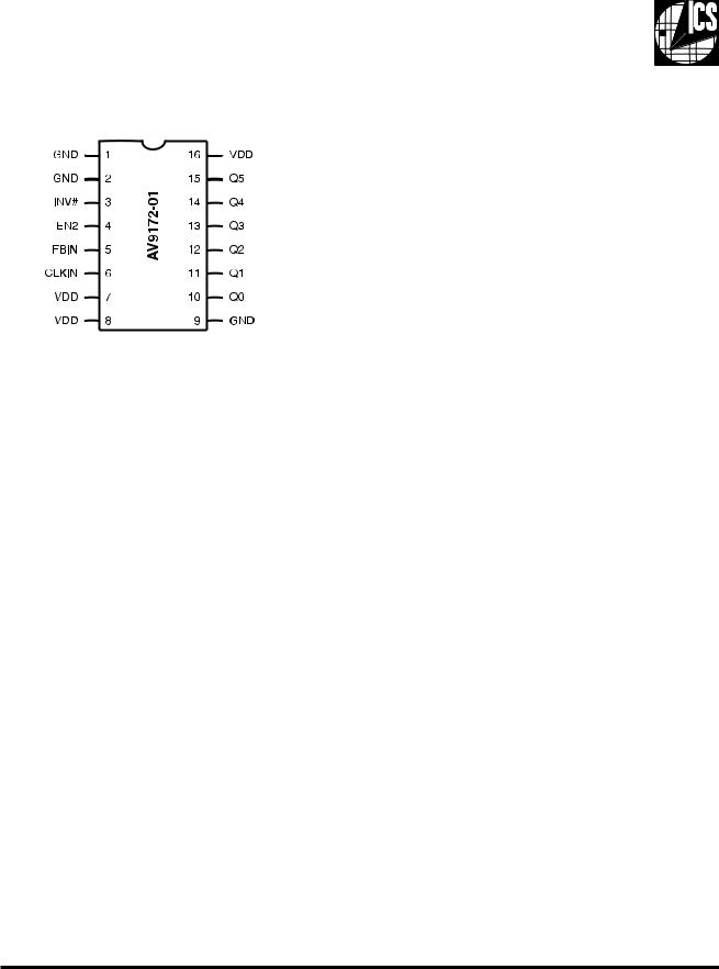
Pin Configuration |
Functionality Table for AV9172-01 |
||
16-Pin SOIC or 16-Pin PDIP
Pin Description for AV9172-01
CLKIN input frequency range 10 to 50 MHz.
EN2 |
INV# |
Q0 |
Q1 |
Q2 |
Q3 |
Q4 |
Q5 |
|
|
|
|
|
|
|
|
0 |
0 |
1X |
1X# |
2X |
2X |
2X |
2X |
0 |
1 |
1X |
1X |
2X |
2X |
2X |
2X |
1 |
0 |
1X |
1X# |
2X |
2X |
1 |
2 |
1 |
1 |
1X |
1X |
2X |
2X |
1 |
2 |
Notes:
1.1X designates that the output is a replica of CLKIN.
2.2X designates that the output is twice the frequency of CLKIN, and in phase.
3.1X# means that the output is at the same frequency and 180°C out of phase (inverted) from CLKIN.
4.Ø1 will produce a ¼ duty cycle clock of CLKIN.
5.Ø2 will produce a ¼ duty cycle clock delayed 180° from CLKIN.
PIN NUMBER |
PIN NAME |
TYPE |
DESCRIPTION |
|
|
|
|
1 |
GND |
- |
GROUND. |
2 |
GND |
- |
GROUND. |
|
|
|
|
3 |
INV# |
Input |
INV# Inverts Q1 when low. (-01 [divisor select -03, -07]) |
4 |
EN |
Input |
EN converts Q4 and Q5 to phase clocks when high. |
|
|
|
|
5 |
FBIN |
Input |
FEEDBACK INPUT from output Q0. |
|
|
|
|
6 |
CLKIN |
Input |
INPUT for reference clock. |
7 |
VDD |
- |
Power supply (+5V). |
|
|
|
|
8 |
VDD |
- |
Power supply (+5V). |
9 |
GND |
- |
GROUND. |
|
|
|
|
10 |
Q0 |
Output |
Q0 phase and frequency same as input (1X). Feed back to pin 5. |
11 |
Q1 |
Output |
Q1 is a 1x clock in phase or 180° out of phase with input. |
|
|
|
|
12 |
Q2 |
Output |
Q2 twice the frequency of Q0 (2x). |
|
|
|
|
13 |
Q3 |
Output |
Q3 twice the frequency of Q0 (2x). |
|
|
|
|
14 |
Q4 |
Output |
Q4 is either a 2X clock or a two-phase clock - see configuration table. |
15 |
Q5 |
Output |
Q5 is either a 2X clock or a two-phase clock - see configuration table. |
|
|
|
|
16 |
VDD |
- |
Power supply (+5V). |
|
|
|
|
2

AV9172
Timing Diagrams for AV9172-01
3
 Loading...