

ICST ICS9159M-20 Datasheet
Integrated
ICS9159-20
Circuit
Systems, Inc.
Frequency Generator for SIS551X and SIS6205 Chip Set Systems
General Description
The ICS9159-20 is a low-cost frequency generator designed
specifically for SIS551X chip set and SIS6205 V GA controller. The integrated buffer minimizes skew. A 14.31818 MHz
XTAL oscillator provides the reference clock to generate
standard Pentium™ frequencies. The CPU clock makes gradual frequency transitions without violating the PLL timing
of internal microprocessor clock multipliers.
Both synchronous and asynchronous bus designs are supported. For chip sets that require an early CPU clock, the
buffers are driven by the CPU clock. In this configuration, the
CPU clock becomes the early clock and the output of the
uncommitted buffers become the bus synchronized bus clocks.
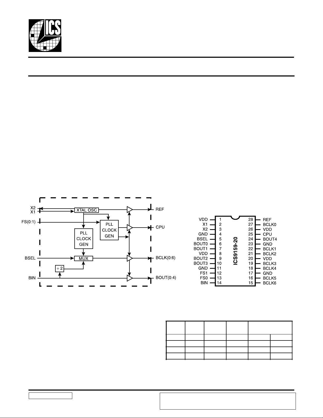
Block Diagram
Features
• One selectable CPU clocks operate up to 66.66 MHz
• 5 uncommitted buffers
• Maximum CPU jitter of ±200ps
• 7 BUS clocks support sync or async bus operation
• 500ps skew window for all synchronous clock edges
• Integrated buffer outputs drive up to 30pF loads
• 3.1V - 3.5V supply range
• 28-pin 300-mil SOIC package
• Supports chip sets requiring early CPU clocking
Applications
• Ideal for green Pentium and P6 PCI systems based on the
SIS5596 chip set
Pin Configuration
9159-20 Rev B 040597
28-Pin SOIC
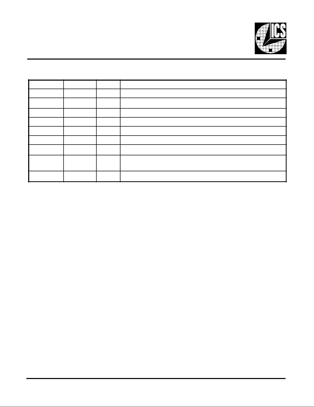
Functionality
3.3V±10%, 0-70°C
Crystal (X1, X2) = 14.318181 MHz
FS1 FS0
0 0 Tistate Tristate Tristate Tristate
0 1 14.318 50 25 33.33
1 0 14.318 60 30 33.33
1 1 14.318 66.66 33.33 33.33
All frequencies in MHz, assuming 14.318 MHz input.
ICS reserves the right to make changes in the device data identified in this publication
without further notice. ICS advises its customers to obtain the latest version of all
device data to verify that any information being relied upon by the customer is current
and accurate.
REF
(MHz)
CPU
(MHz)
Pentium is a trademark of Intel Corporation.
BCLK (MHz)
BSEL=1 BSEL=0
ICS9159-20
Pin Descriptions
PIN NUMBER PIN NAME TYPE DESCRIPTION
1, 8, 20, 26 VDD PWR Power for logic, PCLK and fixed frequency output buffers.
2X1IN
3 X2 OUT XTAL output which includes XTAL load capacitance.
4, 11, 17, 23 GND PWR Ground for logic, PCLK and fixed frequency output buffers.
5 BSEL IN The DISK controller clock is fixed at 33 MHz (with 14.318 MHz input).
6, 7, 9, 10, 24 BOUT(0:4) OUT Uncommitted clock buffer outputs.
13, 12 FS(0:1) IN
15, 16, 18, 19,
21, 22, 27
28 REF OUT
BCLK(0:6) OUT
XTAL or external reference frequency input. This input includes XTAL load
capacitance and feedback bias for a 12 - 16 MHz crystal, nominally 14.31818 MHz.
Frequency multiplier select pins. See table above. These inputs have internal pull-up
devices. 14 BIN IN Uncommitted buffered inputs.
Bus clock outputs are fixed at 33.3 MHz or one half the CPU frequency. 25 CPU
OUT Processor clock outputs which are a multiple of the input reference frequency
as shown in the table above.
REF is a buffered copy of the crystal oscillator or reference input clock,
nominally 14.31818 MHz.
Note: BCLK buffers cannot be supplied with 5 volts (Pins 14 and 20) if CPU and fixed frequencies (Pins 1, 8 and 26) are being
supplied with 3.3 volts.
2
 Loading...