

Integrated
ICS9159-14
Circuit
Systems, Inc.
Frequency Generator and Integrated Buffer for PENTIUM™
General Description
The ICS9159-14 generates all clocks required for high speed
RISC or CISC microprocessor systems such as 486, Pentium,
PowerPC,Ô etc. Four different reference frequency multiplying factors are externally selectable with smooth frequency
transitions. These multiplying factors can be customized for
specific applications.
High drive BCLK outputs provide typically greater than 1V/
ns slew rate into 30pF loads. PCLK outputs provide typically
better than 1V/ns slew rate into 20pF loads while maintaining
±5% duty cycle.
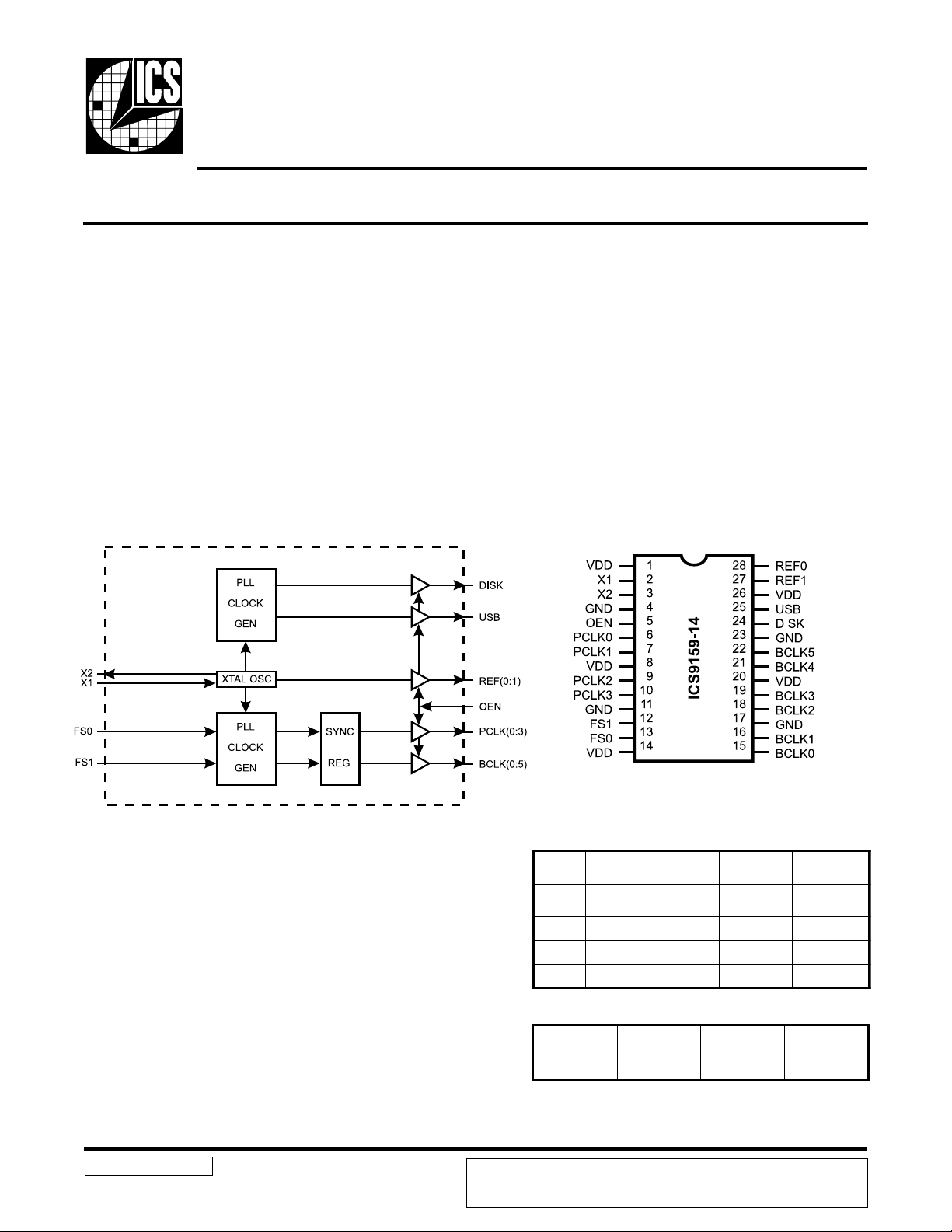
Block Diagram
Features
• Generates up to four processor and six bus clocks, plus
disk, USB and reference clocks
• Synchronous clocks skew matched to 250ps window on
PCLKs and 500ps window on BCLKs
• 3.0V - 5.5V supply range
• 28-pin SOIC package
Pin Configuration
9159-14 Rev B 3/16/00
28-Pin SOIC
Functionality
1SF0SFOCV*
00
01 1Xx7/56813.41)5.66(6.66
10 1Xx11/29813.41)9.95(06
11 1Xx9/96813.41)9.45(55
*VCO range is limited from 60 - 200 MHz.
)3:0(KLCP)5:0(KLCBBSUKSID
2/OCV2/KLCPzHM84zHM42
All frequencies in MHz, assuming 14.318 MHz input.
ICS reserves the right to make changes in the device data identified in this publication
without further notice. ICS advises its customers to obtain the latest version of all
device data to verify that any information being relied upon by the customer is current
and accurate.
x71/811
1X
Pentium is a trademark of Intel Corporation.
PowerPC is a trademark of Motorola Corporation.
FER,1X
)zHM(
813.41)7.94(05
UPC
)zHM(
ICS9159-14
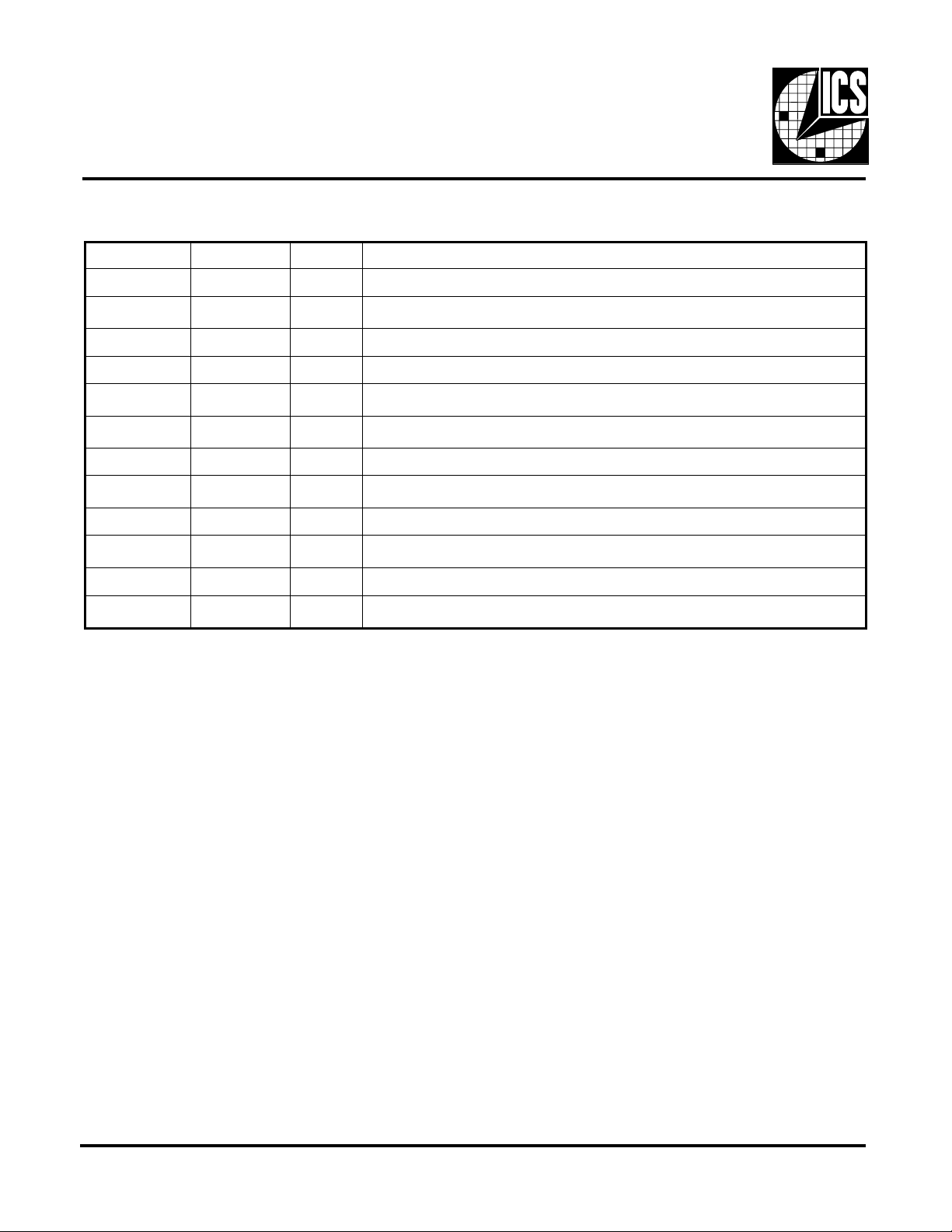
Pin Descriptions
REBMUNNIPEMANNIPEPYTNOITPIRCSED
62,8,1DDVRWP.sreffubtuptuoycneuqerfdexifdnaUPC,cigolrofrewoP
21XNI
32XTUO.ecnaticapacdaolLATXsedulcnihcihwtuptuoLATX
32,11,4DNGRWP.sreffubtuptuoycneuqerfdexifdnaUPC,cigolrofdnuorG
01,9,7,6)3:0(KLCPTUO
21,31)1:0(SFNI
02,41DDVRWP.sreffubtuptuoKLCBrofrewoP
,9181,61,51
22,12
71DNGRWP.sreffubtuptuoKLCBrofdnuorG
5NEONI
52BSUTUO.)tupnizHM813.41htiw(zHM84tadexifsikcolcBSUehT
72,82)1:0(FERTUO
daolLATXsedulcnitupnisihT.tupniycneuqerfecnereferlanretxeroLATX
.zHM81813.41yllanimon,latsyrczHM61-21arofsaibkcabdeefdnaecnaticapac
saycneuqerfecnerefertupniehtfoelpitlumaerahcihwstuptuokcolcrossecorP
.evobaelbatehtninwohs
pu-lluplanretnievahstupniesehT.evobaelbateeS.sniptcelesreilpitlumycneuqerF
.secived
)5:0(KLCBTUO.ycneuqerfKLCPehtflahenotadexiferastuptuokcolcsuB
42.ecivedpu-lluplanretninasahtupnisihT.wolnehwstuptuollasetatsirtNEO
.)tupnizHM813.41htiw(zHM42tadexifsikcolcrellortnocKSIDehTTUOKSID
yllanimon,kcolctupniecnereferrorotallicsolatsyrcehtfoypocdereffubasiFER
.zHM81813.41
2
ICS9159-14
Absolute Maximum Ratings
Supply Voltage.......................................................................................................... 7.0 V
Logic Inputs ....................................................................... GND –0.5 V to V
Ambient Operating Temperature .............................................................0°C to +70°C
Storage Temperature........................................................................... –65°C to +150°C
Stresses above those listed under Absolute Maximum Ratings may cause permanent damage to the device. These ratings
are stress specifications only and functional operation of the device at these or any other conditions above those listed
in the operational sections of the specifications is not implied. Exposure to absolute maximum rating conditions for
extended periods may affect product reliability.
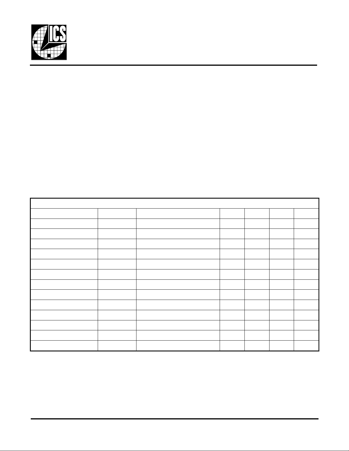
Electrical Characteristics at 3.3V
V
= 3.0 – 3.7 V, TA = 0 – 70°C unless otherwise stated
DD
scitsiretcarahCCD
+0.5 V
DD
RETEMARAPLOBMYSSNOITIDNOCTSETNIMPYTXAMSTINU
egatloVwoLtupnIVLI--V2.0DDV
egatloVhgiHtupnIVHIV7.0DD- - V
tnerruCwoLtupnIILIVNIV0=0.82-5.01--Am
tnerruChgiHtupnIIHIVNIV=DD0.5--0.5Am
1
tnerruCwoLtuptuO
1
tnerruChgiHtuptuO
1
tnerruCwoLtuptuO
1
tnerruChgiHtuptuO
1
egatloVwoLtuptuO
1
egatloVhgiHtuptuO
1
egatloVwoLtuptuO
1
egatloVhgiHtuptuO
ILOVLOseSUB&sUPCrof;V8.0=0.030.74-Am
IHOVHOseSUB&sUPCrof;V0.2=-0.66-0.24-Am
ILOVLOsKLCdexifrof;V8.0=0.520.83-Am
IHOVHOsKLCdexifrof;V0.2=-0.74-0.03-Am
VLOILOseSUB&sUPCrof;Am51=-3.04.0V
VHOIHOseSUB&sUPCrof;Am03-=4.28.2-V
VLOILOsKLCdexifrof;Am5.21=-3.04.0V
VHOIHOsKLCdexifrof;Am02-=4.28.2-V
tnerruCylppuSIDDdedaolnustuptuolla;zHM5.66@-55011Am
Note 1: Parameter is guaranteed by design and characterization. Not 100% tested in production.
3
 Loading...