

Integrated
Circuit
Systems, Inc.
ICS9159-07
Frequency Generator for NexGen
General Description
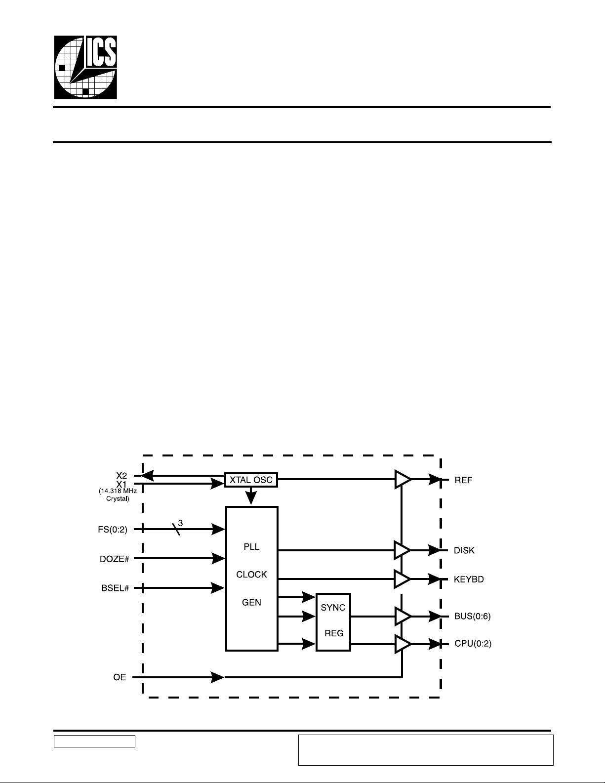
The ICS9159-07 is a low-cost frequency generator designed
specifically for NexGen Nx586 systems. The integrated
buffer minimizes skew and provides the CPU clocks required
by the NexGen Nx586 microprocessor. A 14.318 MHz
XTAL oscil-lator provides the reference clock to generate
standard Nx586 frequencies. The CPU clock makes gradual
frequency transi-tions without violating the PLL timing of
internal microproc-essor clock multipliers.
Either synchronous (2XCPU/3) or asynchronous (32 MHz)
PCI bus operation can be selected. Green PC systems are
supported through doze mode.
Features
• Three CPU clocks operate up to 65 MHz at 3.3V, plus
smooth transitions
• Selection of nine frequencies, tristate
• Seven BUS clocks support sync or async bus
operation
• Integrated buffer outputs drive up to 10pF loads
• 3.13 to 5.25V (3.3±5%, 5.0±5%) supply range
• 28-pin SOIC package
• Clock duty cycles 45/55
Applications
• Ideal for NexGen Nx586 PCI-based motherboard designs
™
Nx586 Systems
Block Diagram
9159-07 Rev C 060697
NexGen is a trademark of NexGen Corporation.
ICS reserves the right to make changes in the device data identified in this publication
without further notice. ICS advises its customers to obtain the latest version of all
device data to verify that any information being relied upon by the customer is current
and accurate.

ICS9159-07
Pin Configuration
28-Pin SOIC
Pin Descriptions
PIN NUMBER PIN NAME TYPE DESCRIPTION
1X1 IN
2 X2 OUT XTAL output which includes XTAL load capacitance.
6,7, 9 CPU(0:2) OUT
3, 11, 23 GND PWR Device Ground.
4, 5, 14 FS(0:2) IN
8, 26 VDD PWR Positive power supply.
10 OE IN Output Enable. All outputs tristate when low.**
12 DOZE# IN Reduces CPU clock frequency to 10 MHz when at a logic low leve l.*
13 BSEL# IN Synchronous and non-synchronous bus clock selector.* ASYNC=0, SYNC=1
15, 16, 18 19,
21, 22, 27
20 V
17 GNDB PWR
24 DISK OUT Fixed 24 MHz clock (with 14. 318 MHz input).
25 KEYBD OUT Fixed 12 MHz clock (with 14.318 MHz input).
28 REF OUT
BCLK(0:6) OUT Bus clock outputs are fixed at 2 ¤3 the PCLK frequency.
B PWR Power for BUS output buffers.
DD
XTAL or external reference frequency input. This input includes XTAL load
capacitance and feedback bias for a 12 - 16 MHz XTAL. Normally, 14.318 MHz.
Processor clock outputs which are a multiple of the input reference frequency as
shown in the table below.
Frequency multiplier select pins. See table below. These inputs have internal pullup devices.*
This ground return path is brought on separately to permit separating the noise
impulses from high output buffers from affecting sensitive internal circuitry.***
REF is a buffered copy of the crystal oscillator or reference input clock,
nominally 14.31818 MHz.
* Internally pulled-up.
** External pull-up resistor of 5 to 20 kW recommended due to dynamic coupling of adjacent CPU pins.
*** Ground for bus clock buffers.
2
ICS9159-07
Functionality
14.318 MHz Input, all frequencies in MHz.
OE FS2 FS1 FS0 DZE CPU (0:2)
1000165 43.3 32
1001160 40 32
1010155.5 37 32
1011151 34 32
1100146.5 31 32
1101142 28 32
1110137.5 25 32
1111135 23.3 32
1XXX010 6.6 32
0 X X X X Tristate Tristate Tristate
BSEL=1 BSEL=0
BUS 0:6
Actual CPU Frequencies
CPU Frequency (MHz) Actual Frequency (MHz)
65 64.98
60 60.03
55.5 55.50
51 51.00
46.5 46.53
42 42.00
37.5 37.48
35 35.00
10 10.00
Tristate Tristate
3
 Loading...