

ICST ICS9159M-05, ICS9159N-05 Datasheet
Integrated
Circuit
Systems, Inc.
General Description
Features
ICS9159-05
Frequency Generator for Pentium
™
/OPTi VIPER Systems
9159-05 Rev F 9/29/98
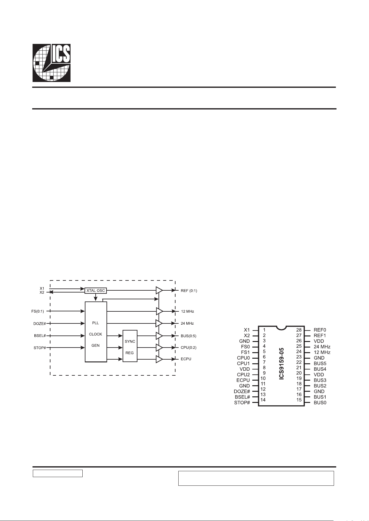
Block Diagram
The ICS9159-05 is a low cost frequency generator designed
specifically for Pentium/Pentium Pro systems. The integrated
buffer minimizes skew and provides the early CPU clock required
by some chipsets such as the OPTi VIPER. A 14.318 MHz
XTAL oscillator provides the reference clock to generate
standard Pentium frequencies. The CPU clock makes gradual
frequency transitions without violating the PLL timing of
internal micro-processor clock multipliers.
The synchronous bus frequencies are selectable as CPU for
local bus or CPU/2 for PCI bus support. Green PC systems
are supported through power-down, doze, and glitch-free
stop clock modes.
• Four CPU clocks operate up to 66.6 MHz at 3.3V with
glitch-free start and stop plus smooth transitions
• 3-6ns early CPU clock supports OPTi VIPER systems
• Selection of 6 frequencies, tristate, or power-down
• Six BUS clocks support local PCI bus operation
• Skew window between synchronous outputs
• Integrated buffer outputs drive up to 30pF loads
• 3.0V - 3.7V supply range
• 28-pin DIP or 28-pin 300-mil SOIC package
Pentium is a trademark of Intel Corporaton.
PowerPC is a trademark of Motorola Corporation.
Applications
• Ideal for green Pentium/Pentium Pro and 486 PCI
systems such as Pentium, PowerPC etc.
ICS reserves the right to make changes in the device data identified in this publication
without further notice. ICS advises its customers to obtain the latest version of all
device data to verify that any
28-Pin 300-mil SOIC
Pin Configuration
2
ICS9159-05
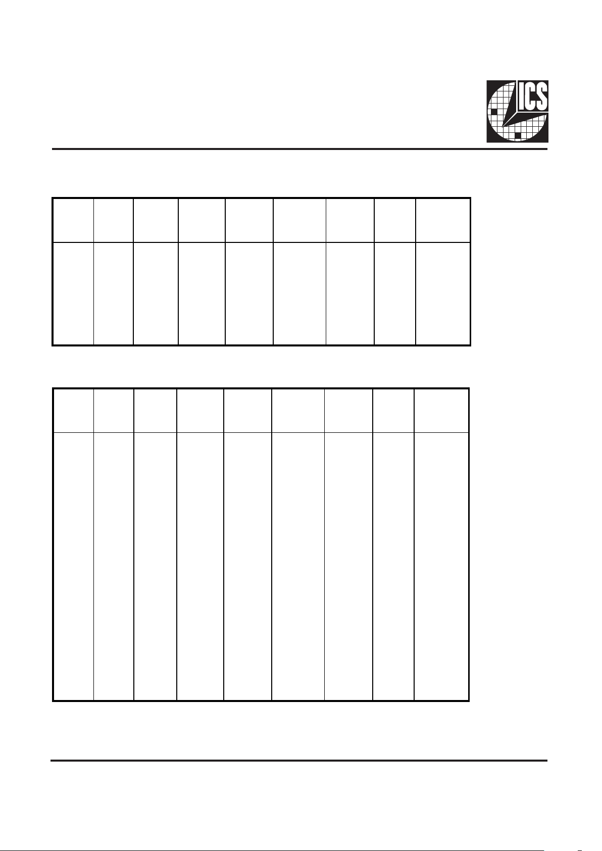
Functionality
Assuming 14.318 MHz input, all frequencies
in MHz. 14 MHz=14.318 MHz
Notes:
1. 000 mode powers-down the PLL sections and forces the outputs low. To ensure glitch-free start and
stop of the CPU and BUS clocks, enter 000 from 001 and exit 000 through 001.
2. Select is FS0, Fs1 = 00, 01, 10, 11.
3. F is the value of CPU, ECPU & BUS. F value is 66.6, 60, 50 or 33.3 as selected by FS(0:1).
Notes:
1. Where F is Frequency selected by FS (0:1)
2. F value is 66.6, 60, 50 or 33.3.
STOP# BSEL# DOZE# FS0 FS1
CPU (0:2)
(MHz)
ECPU
(MHz)
BUS
(0:5)
(MHz)
FIXED
(MHz)
1
1
1
1
0
0
0
0
0
1
0
1
1
0
0
1
1
1
0
0
1
1
0
0
X
X
X
X
Select
X
X
X
X
X
X
X
Select
X
X
X
F
F
F/2
F/2
Stop
Stop
Low
Tristate
F
F
F/2
F/2
Run
Stop
Low
Tristate
F
F
F/4
F/2
Run
Stop
Low
Tristate
24, 12, 14
24, 12, 14
24, 12, 14
24, 12, 14
24, 12, 14
24, 12, 14
L, L, 14
Tristate
STOP# BSEL# DOZE# FS0 FS1
CPU (0:2)
(MHz)
ECPU
(MHz)
BUS
(0:5)
(MHz)
FIXED
(MHz)
1
1
1
1
1
1
1
1
1
1
1
1
1
1
1
1
1
1
0
0
0
1
0
0
0
0
0
1
1
1
1
0
0
0
0
1
1
1
1
1
1
1
0
0
1
1
1
1
1
1
1
1
1
1
0
0
0
0
0
0
0
0
1
0
1
1
0
1
0
0
0
1
1
0
0
1
1
0
0
1
1
0
0
1
1
Select
2
Select
2
Select
2
X
X
X
0
1
0
1
0
1
0
1
0
1
0
1
0
1
0
1
Select
2
Select
2
Select
2
X
X
X
66.6
60
50
33.3
66.6
60
50
33.3
33.3
30
25
16.7
33.3
30
25
16.7
F
3
F/2
Stop
Stop
Low
Tristate
66.6
60
50
33.3
66.6
60
50
33.3
33.3
30
25
16.7
33.3
30
25
16.7
F
3
F/2
Run
Stop
Low
Tristate
33.3
30
25
16.7
66.6
60
50
33.3
16.7
15
12.5
8.3
33.3
30
25
16.7
F
3
F/2
Run
Stop
Low
Tristate
24, 12, 14
24, 12, 14
24, 12, 14
24, 12, 14
24, 12, 14
24, 12, 14
24, 12, 14
24, 12, 14
24, 12, 14
24, 12, 14
24, 12, 14
24, 12, 14
24, 12, 14
24, 12, 14
24, 12, 14
24, 12, 14
24, 12, 14
24, 12, 14
24, 12, 14
L, L, 14
L, L, 14
Tristate
3
ICS9159-05
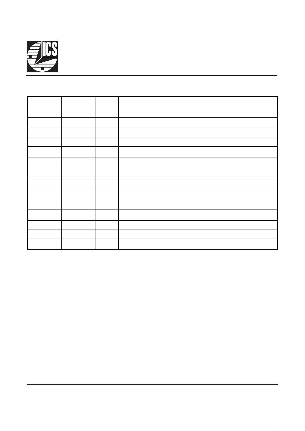
Pin Descriptions
Note:
1. Internally pulled-up
PIN
NUMBER
PIN NAME TYPE DESCRIPTION
8, 20, 26 VDD PWR Power for logic, C PU and fixed frequency output buffers.
1X1 IN
XTA L o r ext e rna l r efe r enc e f r equ e n cy inp u t . This inp ut inc lude s X TA L lo ad
capacitance and feedback bias for a 4-20 MHz XTAL, normally 14.318 MHz.
2 X2 O UT XTAL output which includes XTAL load ca p ac itance .
3, 11, 23, 17 GND PWR Ground for logic, CPU and fixed frequency output buffers.
6, 7, 9 CPU(0:2) OUT
Processor clock outputs which are a multiple of the input reference frequency as
shown in the ta ble.
4, 5 FS(0:1) IN
Frequency multiplier select pins. See table below. These inputs have internal pullup d e vic e s .
10 ECPU OUT Early CPU clock. Transition precedes CPU clocks.
15, 16, 18,
19,21, 22
BUS(0:5) OUT Bus clock outputs are fixed at 1/2 the PCLK frequency.
12 DOZE#
1
IN Doze mode control. Reduces CPU and BUS clock frequencies by 1/2 when low.
13 BSEL#
1
IN
BUS s e lect for BS EL = 0 , BUS = C P U/ 2
for BSEL = 1, BUS = CPU
14 STOP#
1 Stop Clock. Stops all CPU clock outputs and forces them to a logic low level
synchro nously w ith t he ir ne xt lo w le ve l t r a ns it ion .
24 KEYBD OUT 12 MHz fixed clock (with 14.318 MHz input).
25 DISK OUT 24 MHz fixed clock (with 14.318 MHz input).
27, 28 REF (0:1) OUT
REF is a buffered copy of the crystal oscillator or reference input clock,
nominally 14.31818 MHz.
 Loading...