Integrated
Circuit
Systems, Inc.
General Description Features
ICS9148-60
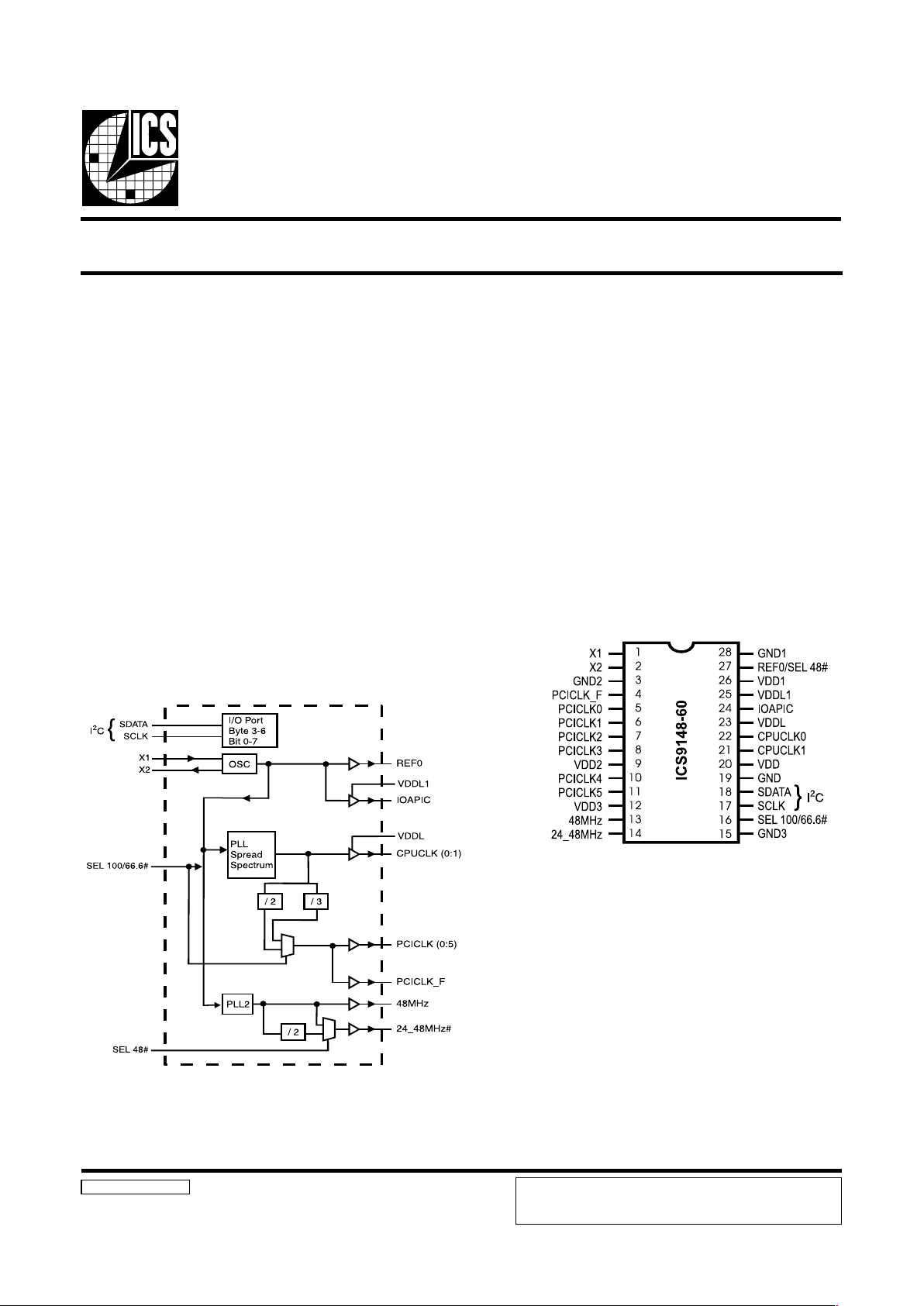
Block Diagram
Pentium/ProTM System Clock Chip
9148-60 Rev D 10/19/99
Pin Configuration
28 pin SOIC and SSOP
Pentium is a trademark on Intel Corporation.
Generates system clocks for CPU, PCI, IOAPIC ,
14.314 MHz, 48 and 24MHz.
Supports single or dual processor systems
Skew from CPU (earlier) to PCI clock 1 to 4ns
Separate 2.5V and 3.3V supply pins
2.5V outputs: CPU, IOAPIC
3.3V outputs: PCI, REF
No power supply sequence requirements
28 pin SOIC and SSOP
Spread Spectrum operation optional for PLL1
CPU frequencies to 100MHz are supported.
The ICS9148-60 is part of a reduced pin count two-chip clock
solution for designs using an Intel BX style chipset.
Companion SDRAM buffers are ICS9179-11 and 12.
There are two PLLs, with the first PLL capable of spread
spectrum operation. Spread spectrum typically reduces system
EMI by 8-10dB. The second PLL provides support for USB
(48MHz) and 24MHz requirements. CPU frequencies up to
100MHz are supported.
The I
2
C interface allows stop clock programming, frequency
selection, and spread spectrum operation to be programmed.
Clock outputs include two CPU (2.5V or 3.3V), seven PCI
(3.3V), one REF (3.3V), one IOAPIC (2.5V or 3.3V), one 48MHz,
and one selectable 48_24MHz.
Ground Groups
GND = Ground Source Core
GND1 = REF0, X1, X2
GND2 = PCICLK_F, PCICLK (0:5)
GND3=48MHz
GNDL = CPUCLK (0:1)
Power Groups
VDD = Supply for PLL core
VDD1 = REF0, X1, X2
VDD2 = PCICLK_F, PCICLK (0:5)
VDD3 = 48MHz
VDDL = CPUCLK (0:1)
VDDL1=IOAPIC
ICS reserves the right to make changes in the device data identified in
this publication without further notice. ICS advises its customers to
obtain the latest version of all device data to verify that any
information being relied upon by the customer is current and accurate.

2
ICS9148-60
Pin Descriptions
REBMUNNIPEMANNIPEPYTNOITPIRCSED
11XNI
pacdaolFp33lanretnisah,tupnilatsyrCzHM813.41NI_LATX
2Xmorfrotsiserkcabdeefdna
22XTUOFp33pacdaollanretnisah,tuptuolatsyrCTUO_LATX
32DNGRWPstuptuoICProfdnuorG
4F_KLCICPTUOtuptuoICPgninnuReerF
11,01,8,7,6,5)5:0(KLCICPTUOV3.3elbitapmocLTT.stuptuokcolcICP
9,62DDVRWPV3.3yllanimon,stuptuoKLCICProfrewoP
213DDVRWPzHM84rofreoP
31zHM84TUOzHM84@tuptuoKLCdexiF
41zHM84_42TUO
fizHM84,purewopta1=72nipfizHM42;tuptuoKLCdexiF
.purewopta0=72nip
513DNGRWPzHM84rofdnuorG
61#6.66/001LESNI
zHM6.66rozHM001gnilbanerofniptceleS
)zHM3.33suonorhcnyssyawlaICP(zHM6.66=L,zHM001=H
71KLCSNIIroftupnikcolC
2
tupniC
81ATADSNIIroftupniataD
2
tupniC
91DNGRWP)1:0(KLCUPCrofdnuorG
02DDVRWPerocLLProfrewoP
22,12)0:1(KLCUPCTUOV5.2yllanimonstuptuokcolctsoHdnaUPC
32LDDVRWPV5.2yllanimon,stuptuoUPCrofrewoP
42CIPAOITUO.zHM813.41tuptuokcolcCIPAOI
52LDDVRWPCIPAOIrofrewoP
621DDVRWP.stuptuoFERrofrewoP
72
0FERTUO.kcolczHM813.41
#84LESNIzHM84si41nip,wolnehW.purewoptatupnidehctaL/tuptuO
821DNGRWP.2X,1X,stuptuoFERrofdnuorG

3
ICS9148-60
1. The ICS clock generator is a slave/receiver, I2C component. It can read back the data stored in the latches for verification.
Read-Back will support Intel PIIX4 "Block-Read" protocol.
2. The data transfer rate supported by this clock generator is 100K bits/sec or less (standard mode)
3. The input is operating at 3.3V logic levels.
4. The data byte format is 8 bit bytes.
5. To simplify the clock generator I2C interface, the protocol is set to use only "Block-Writes" from the controller. The
bytes must be accessed in sequential order from lowest to highest byte with the ability to stop after any complete byte
has been transferred. The Command code and Byte count shown above must be sent, but the data is ignored for those
two bytes. The data is loaded until a Stop sequence is issued.
6. At power-on, all registers are set to a default condition, as shown.
General I2C serial interface information
The information in this section assumes familiarity with I2C programming.
For more information, contact ICS for an I2C programming application note.
How to Write:
Controller (host) sends a start bit.
Controller (host) sends the write address D2
(H)
ICS clock will acknowledge
Controller (host) sends a dummy command code
ICS clock will acknowledge
Controller (host) sends a dummy byte count
ICS clock will acknowledge
Controller (host) starts sending first byte (Byte 0)
through byte 5
ICS clock will acknowledge each byte one at a time.
Controller (host) sends a Stop bit
How to Read:
Controller (host) will send start bit.
Controller (host) sends the read address D3
(H)
ICS clock will acknowledge
ICS clock will send the byte count
Controller (host) acknowledges
ICS clock sends first byte (Byte 0) through byte 6
Controller (host) will need to acknowledge each byte
Controller (host) will send a stop bit
Notes:
Controller (Host) ICS (S lave/Receiver)
Start Bit
Address
D2
(H)
AC
K
Dummy C ommand Co de
AC
K
Dummy Byte Count
AC
K
Byte 0
ACK
Byte 1
AC
K
Byte 2
AC
K
Byte 3
ACK
Byte 4
AC
K
Byte 5
AC
K
Byte 6
ACK
Stop Bit
How to Write:
Controller (Host) ICS (Slave/Receiver)
Start Bit
Address
D3
(H)
AC
K
Byte Coun
t
ACK
Byte
0
ACK
Byte 1
ACK
Byte
2
ACK
Byte
3
ACK
Byte
4
ACK
Byte
5
ACK
Byte
6
ACK
Stop Bit
How to Read:
 Loading...