

Integrated
Circuit
Systems, Inc.
General Description Features
ICS9147-09
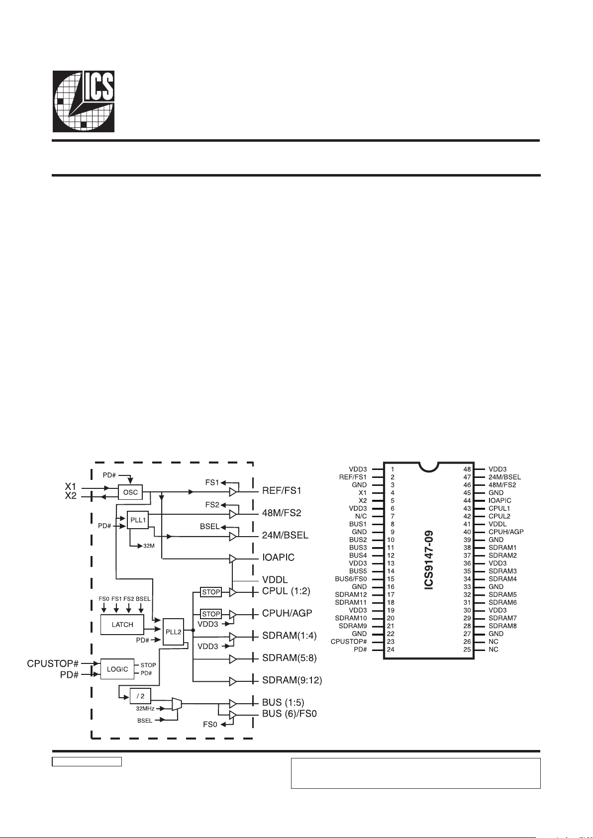
Block Diagram
Pentium is a trademark of Intel Corporation
Frequency Generator & Integrated Buffers for 686 Series CPUs
9147-09 Rev A 10/2897P
Pin Configuration
The ICS9147-09 generates all clocks required for high
speed RISC or CISC microprocessor systems such as Intel
PentiumPro, AMD or Cyrix processors. Four bidirectional I/O
pins (FS0, FS1, FS2, BSEL) are latched at power-on to the
functionality table. The Six BUS clocks can be selected as
either synchronous at 1/2 CPU speed or asynchronous at
32MHz selected by BSEL latched input.The inputs provide
for tristate and test mode conditions to aid in system level
testing.These multiplying factors can be customized for
specific applications. Glitch-free stop clock controls
provided for CPU.
High drive BUS and SDRAM outputs typically provide
greater than 1 V/ns slew rate into 30 pF loads. CPU outputs
typically provide better than 1V/ns slew rate into 20pF
loads while maintaining 50±5% duty cycle. The REF clock
outputs typically provide better than 0.5V/ns slew rates.
Seperate buffer supply pin VDDL allows for nominal 3.3V
voltage or reduced voltage swing (from 2.9 to 2.5V) for
CPUL (1:2) and IOAPIC outputs.
Total of 15 CPU speed clocks:
- Two copies of CPU clock with VDDL (2.5 to 3.3V)
- Twelve (12) SDRAM (3.3v) plus one
CPUH/AGP (3.3V) clocks
Six copies of BUS clock (synchronous with CPU clock/2 or
asynchronous 32 MHz)
250ps output skew window for CPU andSDRAM clocks
and 500ps window BUS clocks. CPU clocks to
BUSclocks skew 1-4ns (CPU early)
Two copies of Ref. clock @14.31818 MHz (One driven
by VDDL as IOAPIC)
One 48 MHz (3.3 V TTL) for USB support and single
24 MHz.
Separate VDDL for CPUL (1:2) clock buffers and
IOAPIC to allow 2.5V output (or Std. Vdd)
3.0V 3.7V supply range w/2.5V compatible outputs
48-pin SSOP package
48-Pin SSOP
ICS reserves the right to make changes in the device data identified in this
publication without further notice. ICS advises its customers to obtain the latest
version of all device data to verify that any information being relied upon by the
customer is current and accurate.
2
ICS9147-09
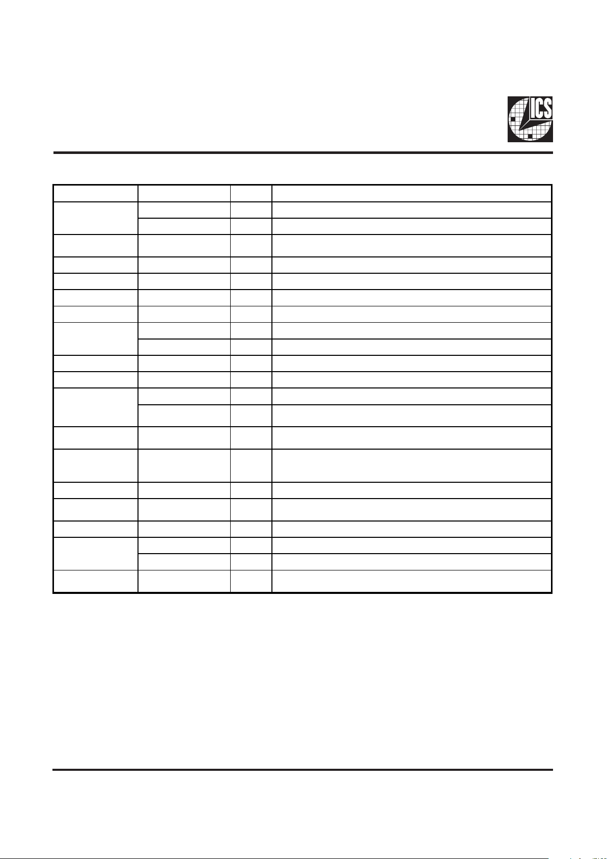
Pin Descriptions
* Bidirectional input/output pins, input logic level determined at internal power-on-reset are latched. Use 10Kohm resistor to
program logic Hi to VDD or GND for logic low.
PIN NUMBER PIN NAME TYPE DESCRIPTION
2
RE F OUT R eference clock output*
FS 1 IN Logic input frequency select Bit1*. Input latched at Poweron.
3, 9, 16, 22,
27, 33, 39, 45
GND PWR Ground.
4 X1 IN Crystal input. Nominally 14.318 MHz. Has internal load cap
5 X2 OUT Crystal output. Has internal load cap and feedack resistor to X1
41 VDDL PWR 2.5 or 3.3V buffer power for CPUL and IOAPIC output buffers.
8, 10, 11, 12, 14, BUS (1:5) OUT B US clock outputs. see select table for frequency
15
BUS6 OUT BUS clock output. See select table for frequency.*
FS0 IN Logic input frequency select Bit0.*. Input latched at Poweron.
23 CPU_STOP# IN Halts CPU Clocks at Logic "0" level when low. Internal Pull-up
24 PD# IN Powers down chip, active low. Internal Pull-up
47
24M O UT 24MHz fixed clock.*
BSEL I N
Logic input* for selecting synchronous or asynchronous BUS
frequency- see table above. Input latched at Poweron.*
1, 6, 13, 19,
30, 36, 48
VDD3 PWR 3.3 volt core logic and buffer power
17, 18, 20, 21, 28,
29, 31, 32, 34,
35, 37, 38
SDRAM (1:12) OUT S DRAM clocks at CPU speed. See select table for frequency.
40 CPUH/AGP OUT CPU clock operates at SDRAM VDD level (3.3V nom), for AGP etc.
42, 43 CPUL (1:2) OU T
CPU clocks .See select table for frequency. Operates at down to
2.5V controlled by VDDL pin.
7, 25, 26 N/C — Pins not internally connected.
46
48 M OUT 48 MHz fixed clock output*.
FS 2 IN Logic input frequency select Bit 2*. Input latched at Poweron.
44 IOAPIC OUT
Reference clock (14.318MHz) powered by VDDL,
operating 2.5 to 3.3V.
3
ICS9147-09
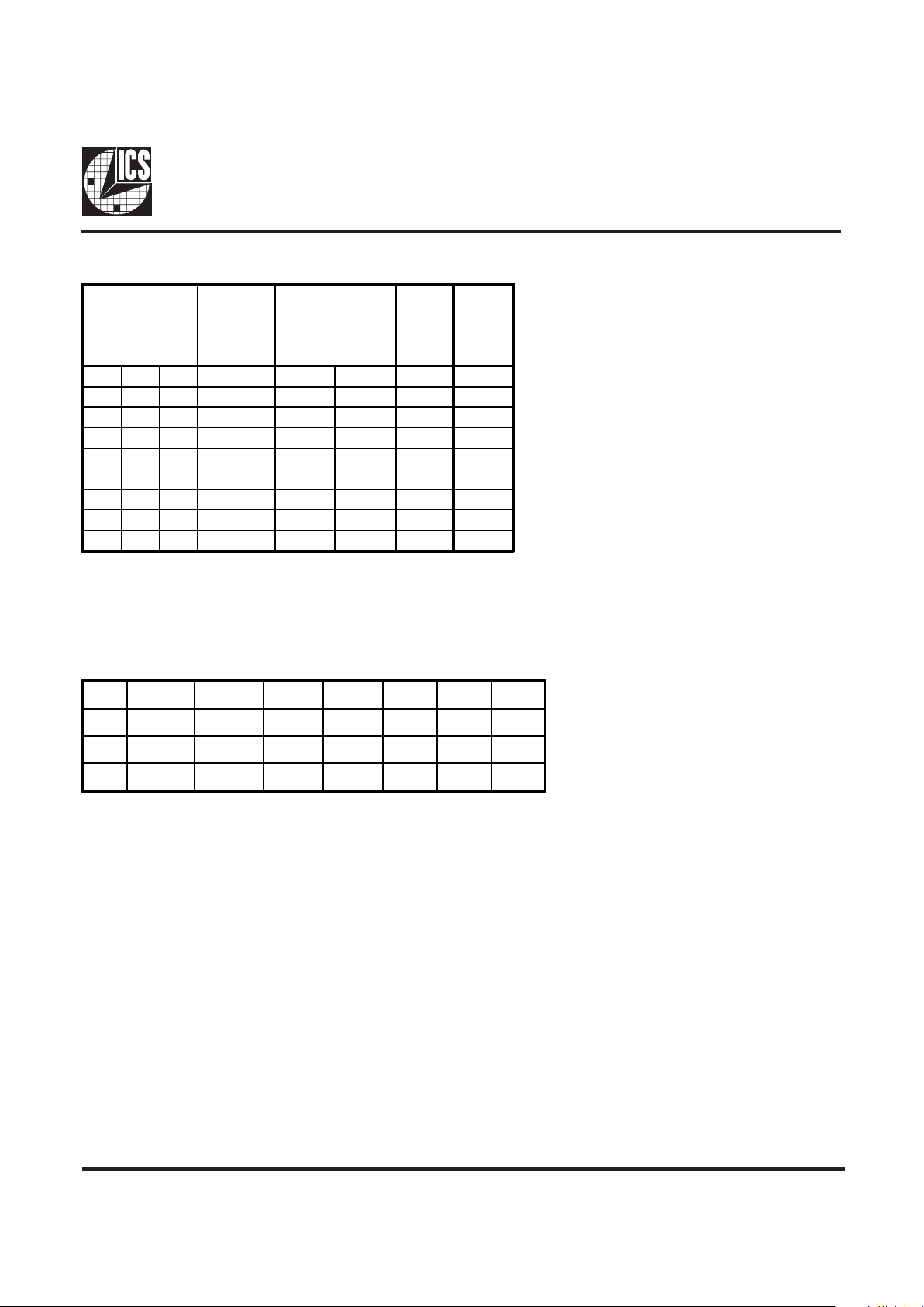
Functionality with (14.31818 MHz input)
Clock Enable Configuration
**Test: is the frequency applied to the X1 input. Can be crystal or tester generated clock overriding crystal at X1 pin.
Address Select
CPUL
(1:2)
CPUH
SDRAM
(1:12)
BUS (1:6)
(MHz)
24M
(MHz)
48M
(MHz)
FS2 FS1 FS0 (MHz) BSEL=1 BSEL=0 (MHz) (MHz)
000 60 30 32 24 48
001 66.8 33.4 32 24 48
010 50 25 32 24 48
011 55 27.5 32 24 48
100 75 37.5 32 24 48
101 68.5 34.3 32 24 48
1 1 0 83.3 41.65 32 24 48
1 1 1 Tristate Tristate Tristate Tristate Tristate
PD# CPUSTOP#
CPUL (1:2)
CPUH
SDRAM
(1:12)
BUS (1:6) 24MHz 48MHz REF
1 1 Running Running Running Running Running Running
1 0 Stop Low Running Running Running Running Running
0 X Stop Low Stop Low Stop Low Stop Low Stop Low Stop Low
4
ICS9147-09
Absolute Maximum Ratings
Electrical Characteristics at 3.3V
Supply Voltage . . . . . . . . . . . . . . . . . . . . . . . . . . 7.0 V
Logic Inputs . . . . . . . . . . . . . . . . . . . . . . . . . . . . GND 0.5 V to VDD +0.5 V
Ambient Operating Temperature . . . . . . . . . . . . 0°C to +70°C
Storage Temperature . . . . . . . . . . . . . . . . . . . . . . 65°C to +150°C
VDD = 3.0 3.7 V, TA = 0 70° C unless otherwise stated
Note 1: Parameter is guaranteed by design and characterization. Not 100% tested in production.
Stresses above those listed under Absolute Maximum Ratings may cause permanent damage to the device. These ratings are
stress specifications only and functional operation of the device at these or any other conditions above those listed in the
operational sections of the specifications is not implied. Exposure to absolute maximum rating conditions for extended
periods may affect product reliability.
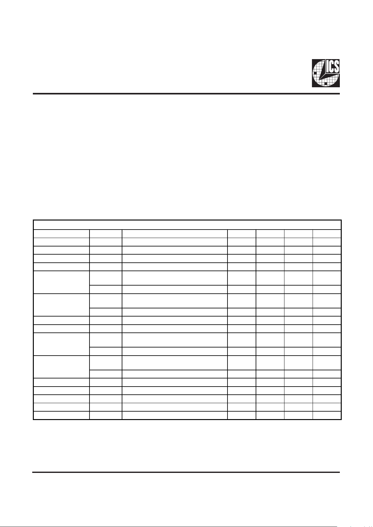
DC Characteristics
PARAMETER SYMBOL TEST CONDITIONS MIN TYP MAX UNITS
Input Low Voltage V
IL Latched inputs and Fulltime inputs - - 0.2VDD V
Input High Voltage V
IH Latched inputs and Fulltime inputs 0.7VDD --V
Input Low Current I
IL VIN = 0V (Fulltime inputs) -28.0 -10.5 - µA
Input High Current I
IH VIN=VDD (Fulltime inputs) -5.0 - 5.0 µ A
Output Low Current
I
OL1a
VOL = 0.8V; CPU, SDRAM IOAPIC, REF,
BUS; V
DD2 = 3.3V
19.0 30.0 - mA
I
OL1b VOL = 0.8V; CPUL, IOAPIC; VDD2 = 2.5V 19.0 30.0 mA
Output High Current
I
OH1a
VOH = 2.0V; CPU, SDRAM IOAPIC, REF,
BUS; V
DD2 = 3.3V
- -26.0 -16.0 mA
I
OH1b VOH = 2.0V; CPUL, IOAPIC; VDD2 = 2.5V -12.5 -9.5 mA
Output Low Current I
OL2 VOL = 0.8V; for fixed 24, 48 16.0 25.0 - mA
Output High Current I
OH2 VOH = 2.0V; for fixed 24, 48 - -22.0 -14.0 mA
Output Low Voltage
V
OL1a
IOL = 10mA; CPU, SDRAM IOAPIC REF,
BUS;V
DD2 = 3.3V
-0.30.4V
V
OL1b IOL = 10mA; CPUL, IOAPIC; V DD2=2.5V 0.3 0.4 V
Output High Voltage
V
OH1a
IOH = -10mA; CPU, SDRAM, IOAPIC,
REF, BUS; V
DD = 3.3V
2.4 2.8 - V
V
OH1b IOH = -10mA; CPUL, IOAPIC; VDD2=2.5V 1.95 2.1 V
Output Low Voltage V
OL2 IOL = 8mA; for fixed 24, 48MHz CLKs - 0.3 0.4 V
Output High Voltage V
OH2 IOH = -8mA; for fixed 24, 48MHz CLKs 2.4 2.8 - V
Supply Current I
DD @66.6 MHz ; all outputs unlo aded - 120 180 mA
Power Down Current I
pd PD#= 0 - 5.0 20.0 µA
Pull-up Resistor R
pu CPUSTOP#; PD# 20 40 80 Kohms

5
ICS9147-09
Electrical Characteristics at 3.3V
VDD = 3.0 3.7 V, TA = 0 70° C unless otherwise stated
Note 1: Parameter is guaranteed by design and characterization. Not 100% tested in production.
AC Characteristics
PARAMETER SYMBOL TEST CONDITIONS MIN TYP MAX UNITS
Rise Time
1
Tr1
20pF load, 0.8 to 2.0V
CPU, SDRAM, BUS & REF
-0.91.5ns
Fall Time
1
Tf1
20pF load, 2.0 to 0.8V
CPU, SDRAM, BUS & REF
-0.81.4 ns
Rise Time
1
Tr3
20pF load, 0.8 to 2.0V
fixed 20 & 48 clocks
-0.91.5 ns
Fall Time
1
Tf3
20pF load, 2.0 to 0.8V
fixed 20 & 48 clocks
-1.11.5 ns
Rise Time
1
Tr4
20pF load, 0.4 to 2.0V , CPUL with
VDDL = 2.5V
-2.02.5 ns
Fall Time
1
Tf4
20pF load, 2.0 to 0.4V, CPUL with
VDDL = 2.5V
-1.62.5 ns
Duty Cycle
1
Dt
20pF load @ VOUT=1. 4V
All clocks except 48MHz and REF
47 52 57 %
Duty Cycle
1
DT2
20pF load @ VOUT=1. 4V
48MHz and REF outputs
40 50 60 %
Jitter, One Sigma
1
Tjis1
CPU & BUS Clocks; Load=20pF,
SDRAM; Load = 30pF, VDDL = 3.3
or 2.5V
FOUT=25 MHz, BSEL=1
-50150 ps
Jitter, Absolute
1
Tjab1
CPU & BUS Clocks; Load=20pF,
SDRAM; Load = 30pF, VDDL = 3.3
or 2.5V
FOUT
≥25 MHz, BSEL=1
-250 - 250 ps
Jitter, One Sigma
1
Tjis2 Fixed CLK; Load=20pF - 1 3 %
Jitter, Absolute
1
Tjab2 Fixed CLK; Load=20pF -5 2 5 %
Jitter, Cycle to Cycle
1
Tcc1 CPU Clocks, Load=20pF BSEL=1 - 250 ps
Jitter, Cycle to Cycle
1
Tcc2
CPU Clocks, Load=20pF BSEL=1
VDDL=2.5V
- 350 ps
Input Freque ncy
1
Fi 12.0 14.318 16.0 MHz
Ratio of nominal to output
frequency
Fout1
With input driven at 14.31818MHz to
20.0, 48.0MHz
-1 -0.1 +1 ppm
Logic Input Ca pacitance
1
CIN Logic input pins - 5 - pF
Crystal Oscillator Capacitance
1, 2
CINX X1, X2 pins 2 4 6 pF
Power-on Time
1
ton
From VDD=1.6V to 1st crossing of
66.6 MHz VDD supply ramp < 40ms
-2.54.5 ms
Clock Skew Window
1
Tsk1
CPU to CPU or SDRAM;
Load=20pF; @1.4V
(Same VDD)
- 150 250 ps
Clock Skew Window
1
Tsk2
BUS to BUS, SDRAM to SDRAM;
Load=20pF; @1.4V
- 300 500 ps
Clock Skew Window
1
Tsk3
CPU to BUS; Load=20pF; @1.4V
(CPU is early)
1.6 2.1 4. 6 ns
Clock Skew Window
1
Tsk4
CPUL to BUS, VDDL=2.5V
Vth=1.25, CPUL (BUS Vth=1.4V )
0.50 1.50 3.0 ns
Clock Skew Window
1
Tsk5
SDRAM, CPUH (@3.3V, Vth=1.4V)
to CPUL (@2.5V Vth=1.25V)
Load=20pF
(2.5V CPUL is late)
100 600 850 ps

6
ICS9147-09
Pins 2, 15, 46 and 47 on the ICS9147-09 serve as dual
signal functions to the device. During initial power-up,
they act as input pins. The logic level (voltage) that is
present on these pins at this time is read and stored into a
4-bit internal data latch. At the end of Power-On reset, (see
AC characteristics for timing values), the device changes
the mode of operations for these pins to an output function.
In this mode the pins produce the specified buffered
clocks to external loads.
To program (load) the internal configuration register for
these pins, a resistor is connected to either the VDD (logic 1)
power supply or the GND (logic 0) voltage potential. A 10
Kilohm(10K) resistor is used to provide both the solid CMOS
programming voltage needed during the power-up
programming period and to provide an insignificant load on
the output clock during the subsequent operating period.
Figs. 1 and 2 show the recommended means of implementing
this function. In Fig. 1 either one of the resistors is loaded
onto the board (selective stuffing) to configure the devices
internal logic. Figs. 2a and b provide a single resistor
loading option where either solder spot tabs or a physical
jumper header may be used.
These figures illustrate the optimal PCB physical layout
options. These configuration resistors are of such a large
ohmic value that they do not effect the low impedance clock
signals. The layouts have been optimized to provide as little
impedance transition to the clock signal as possible, as it
passes through the programming resistor pad(s).
Shared Pin Operation Input/Output Pins
The ICS9147-09 includes a production test verification
mode of operation. This requires that the FS2 and FS1 pins
be programmed to a logic high and the FS0 pin be
programmed to a logic low(see Shared Pin Operation
section). In this mode the device will output the following
frequencies.
Note: REF is the frequency of either the crystal connected
between the devices X1and X2, or, in the case of a device
being driven by an external reference clock, the frequency
of the reference (or test) clock on the devices X1 pin.
Test Mode Operation
Fig. 1
Pin Frequency
REF, IOAPIC REF
48MHz REF/2
24MHz REF/4
CPU, SDRAM REF2
BUS BSEL=1 REF/4
BUS BSEL=0 REF/3

7
ICS9147-09
Fig. 2a
Fig. 2b

8
ICS9147-09
Recommended PCB Layout for ICS9147-09
NOTE:
This PCB Layout is based on a 4 layer board with an internal Ground (common) and VDD plane. Placement of
components will depend on routing of signal trace. The 0.1uf Capacitors should be placed as close as possible
to the Power pins. Placement on the backside of the board is also possible. The Ferrite Beads can be replaced
with 10-15ohm Resistors. For best results, use a Fixed Voltage Regulator between the main (board) VDD and the
different VDD planes.

9
ICS9147-09
Ordering Information
ICS9147F-09
Pattern Number (2 or 3 digit number for parts with ROM code patterns)
Package Type
F=SSOP
Device Type (consists of 3 or 4 digit numbers)
Prefix
ICS = Standard Device
Example:
ICS XXXX F - PPP
SSOP Package
SYMBOL COMMON DIMENSIONS VARIATIONS D N
MIN. NOM. MAX. MIN. NOM. MAX.
A .095 . 101 .110 AC .620 .625 .63 0 48
A1 .008 .012 .016 AD .720 .725 .730 56
A2 .088 .090 .092
B .008 .010 .0135
C.005- .010
D See Variations
E .29 2 .2 96 .299
e0.025 BSC
H .400 .406 .410
h .010 .013 .016
L .024 .032 .040
N See Variations
∝
0° 5° 8°
X .085 . 093 .100
ADVANCE INFORMATION documents contain information on
new products in the sampling or preproduction phase of development. Characteristic data and other specifications are subject to
change without notice.
 Loading...