

Integrated
Circuit
Systems, Inc.
ICS9147-16
Frequency Generator & Integrated Buffers for PENTIUM
General Description Features
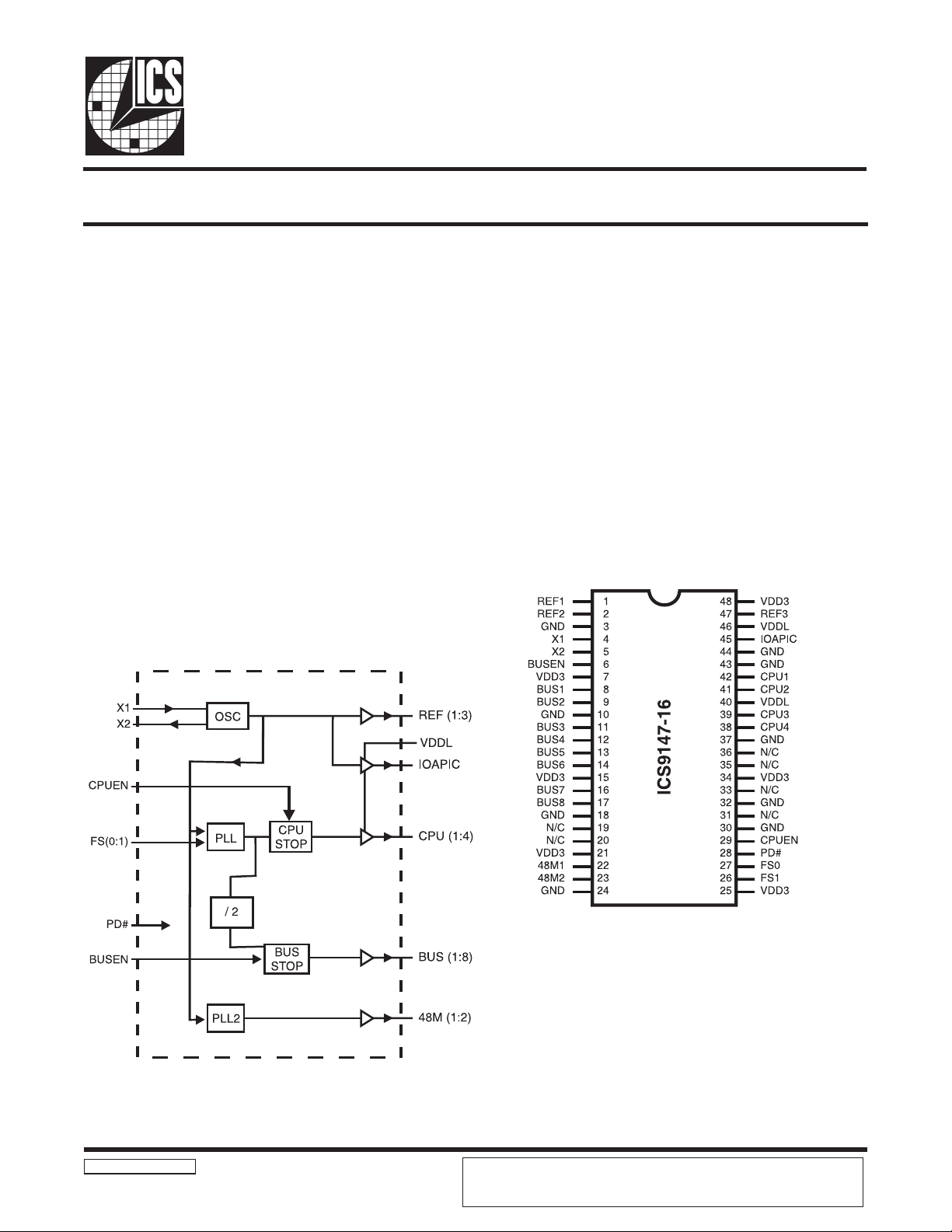
The ICS9147-16 generates all clocks required for high
speed RISC or CISC microprocessor systems such as Intel
PentiumPro. Two different reference frequency multiplying
factors are externally selectable with smooth frequency
transitions. Glitch-free Stop clock control is provided for
CPU and BUS clocks. Complete chip low current mode is
achieved with the Power Down# pin.
High drive BUS outputs typically provide greater than 1 V/
ns slew rate into 30pF loads. CPU outputs typically provide
better than 1V/ns slew rate into 20pF loads while
maintaining
outputs typically provide better than 0.5V/ns slew rates.
Separate buffer supply pins VDDL allow for nominal 3.3V
voltage or reduced voltage swing (from 2.9 to 2.5V) for
CPU (1:4) and IOAPIC outputs.
50±
5% duty cycle. The REF and IOAPIC clock
Block Diagram
Generates four processor, eight bus, four 14.31818
MHz, two 48 MHz clocks for USB support.
CPU to BUS clock skew 1 to 4ns (CPU early)
Synchronous clocks skew matched to 250ps window on
CPU and 500ps window on BUS.
Selectable multiplying ratios
Glitch free stop clock controls CPUEN and BUSEN
3.0V 3.7V supply range, 2.5V to VDD supply range for
CPU (1:4) clocks and IOAPIC clock.
48-pin SSOP package
Pin Configuration
TM
9147-16 Rev A 072897P
48-Pin SSOP
Pentium is a trademark of Intel Corporation
ICS reserves the right to make changes in the device data identified in this
publication without further notice. ICS advises its customers to obtain the latest
version of all device data to verify that any information being relied upon by the
customer is current and accurate.
ICS9147-16
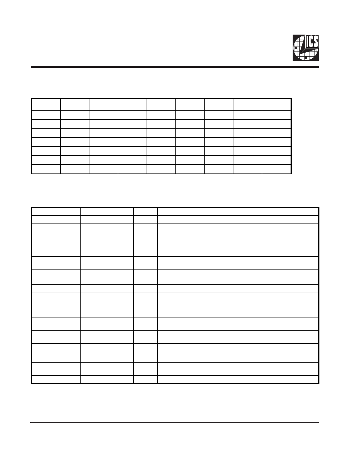
Functionality
PD# BUSEN CPUEN FS1 FS0 CPU (1:4) BUS
11100TristateTristateTristateTristate
11101603014.3181848
1111066.633.314.3181848
11111REF/2REF/4REFREF/2
1 1 0 X X LOW Running 14.31818 48
1 0 1 X X Running LOW 14.31818 48
0XXXXLOWLOWLOWLOW
REF
IOAPIC
Pin Descriptions
PIN NUMBER PIN NAME TYPE DESCRIPTI ON
1, 2, 47 REF1, REF2, REF3 OUT 14.318 MHz reference clock outputs.
3, 10, 18, 24, 30, 32,
37, 43, 44
4X1 IN
5 X2 OUT Crystal output, has internal crystal load capacitor
8, 9, 11, 12, 13, 14,
16, 17
26, 27 FS (0:1) IN Select pin for enabling CPU and BUS clock frequencies.*
7, 15, 21, 25, 34, 48 VDD3 PWR Core and Buffer output clock power supply.
22, 23 48M (1:2) O UT 48 MHz clock output
28 PD# I N
29 CPUE N IN
38, 39, 41, 42 CPU (1:4) OU T
6BUSEN IN
45 IOAPIC OUT
40, 46 VDDL P WR
19, 20, 31, 33, 36 N/C - No connection internally to these pi ns.
GND PWR Ground.
Crystal input, has internal crystal load capacitor, and feedback resistor
from X2. Nominally 14.31818MHz.
BUS (1:8) OUT BUS clock outputs, operates synchronously at CPU/2.
Device power down input, stops outputs low and shuts off crystal
oscillator and PLLs when low.*
Output enable for all CPU clocks, a logic low will Stop low all CPU
clocks.*
CPU clock output clocks, operates at VDDL supply voltage (with
IOAPIC), either nominal 3.3V VDD or reduced voltage 2.9 to 2.5V.
Output enable for all BUS clock, a logic low will stop Low all Bus
clocks.*
IOAPIC clock output. (14.318 MHz), operates at VDDL supply voltage
with CPU (1:4) , either nomi nal 3.3V VDD or red uced voltage
2.9 to 2.5V.
Power supply for CPU and IOAPIC block buffers, operates at nominal
3.3V VDD or reduced voltage 2.9 to 2.5V.
48
(MHz)
* Has internal pull-up to V
DD3
.
2
 Loading...