

Integrated
Circuit
Systems, Inc.
General Description
Features
ICS9120-11
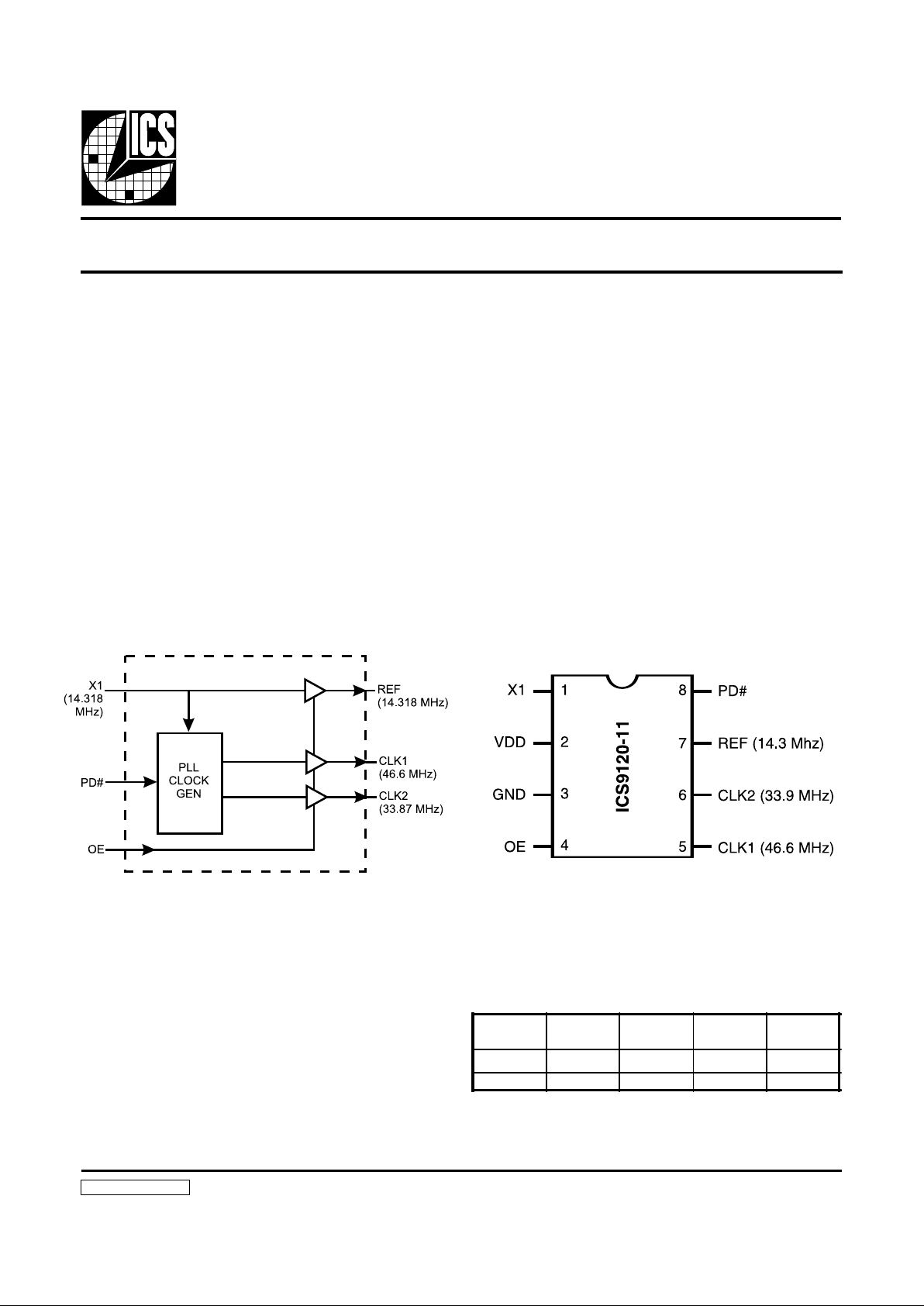
The ICS9120-11 is a high performance frequency generator.
The ICS9120-11 provides high accuracy; low jitter PLLs
meet the 0.20% frequency tolerance and -96dB signal-tonoise ratios. Fast output clock edge rates minimize board
induced jitter.
The ICS9120-11 operates over the entire 3.0 - 5.5V range
and provides power-down to minimize energy consumption.
• Generates 46.6 MHz and 33.868 MHz clocks
• Buffered REFCLK output
• 0.20% frequency accuracy
• 100ps one sigma jitter maintains 16-bit performance
• Output rise/fall times less than 2.5ns
• On-chip loop filter components
• 3.0V - 5.5V supply range
• 8-pin, 150-mil SOIC package Advance Information
9120-11 Rev B 012197
Block Diagram
Frequency Generator for Multimedia Audio Synthesis
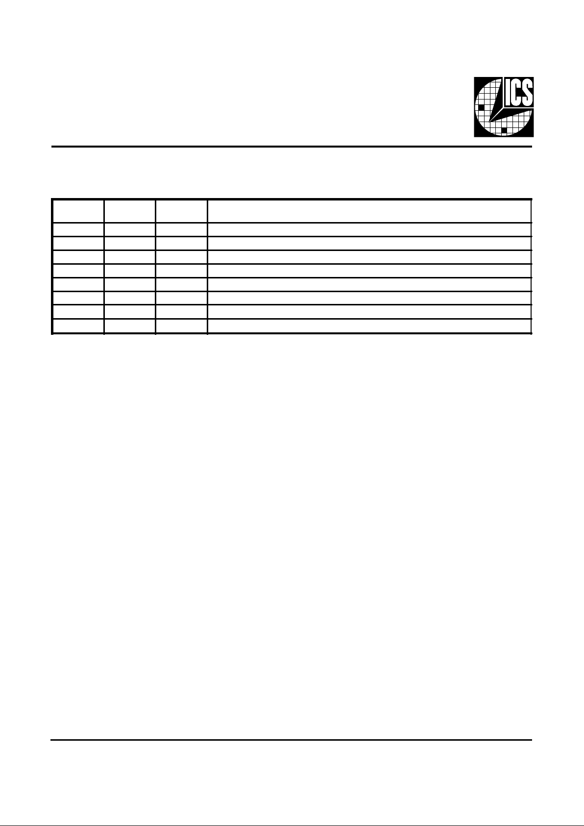
X1 (MHz) PD#
33.9
(MHz)
46.6
(MHz)
14.3
(MHz)
- 0 Low Low Low
14.318 1 33.868 46.6 14.318
Functionality
Note: PD# (Pin 8) and OE (Pin 4) are internally pulled-up
to VDD and therefore may be left disconnected or driven by
open collector logic.
Pin Configuration
8-Pin SOIC
2
ICS9120-11
Pin Descriptions for ICS9120-11
* Pin 1 contains no loading capacitor.
PIN
NUMBER
PIN
NAME
TYPE DESCRIPTION
1 X1 Input External clock source.*
2 VDD Power +Power supply input.
3 GND Power Ground return for Pin 2.
4 OE Input Output Enable (tristates all outputs when at logic low level); has pull-up.
5 CLK1 Input 46.6 MHz clock output.
6 CLK2 Output 33.9 MHz clock output.
7 REF Output 14.318 M Hz reference clock output.
8 PD# Input Power-down input (powers-down entire device when low); has pull-up.

3
ICS9120-11
Absolute Maximum Ratings
AVDD, VDD referenced to GND ......................................................................................................................................... 7V
Operating temperature under bias ....................................................................................................................... 0°C to +70°C
Storage temperature.........................................................................................................................................-65°C to +150°C
Voltage on I/O pins referenced to GND........................................................................................GND -0.5V to VDD +0.5V
Power dissipation.......................................................................................................................................................... 0.5 W atts
Stresses above those listed under Absolute Maximum Ratings ma y cause permanent damage to the de vice. T his is a stress rating
only and functional operation of the device at these or any other conditions above those indicated in the operational sections
of the specifications is not implied. Exposure to absolute maximum rating conditions f or extended periods may affect product
reliability .
Electrical Characteristics at 5V
Operating VDD = +4.5V to +5.5V; TA =0°C to 70°C unless otherwise stated
*Parameter is guaranteed by design and characterization. Not 100% tested in production.
DC Charact eristics
PARAMETER SYMBOL TEST CONDITIONS MIN TYP MAX UNITS
Input Low Voltage V
IL
--0.8V
Input High Voltage V
IH
2.0 - - V
Input Low Current I
IL
VIN=0V -18.0-8.3-µA
Input High Current I
IH
VIN=V
DD
- - 5.0 µA
Output Low Voltage V
OL
*IOL=+10mA - 0.15 0.4 V
Output High Voltage V
OH
*IOH=-30mA 2. 4 3 . 7 - V
Output Low Current I
OL
*VOL=0.8V 25.0 45.0 - mA
Output High Current I
OH
*VOH=2.4V - -53.0 -35.0 mA
Supply Current I
DD
Unloaded - 23.0 50.0 mA
Supply Current,
Power-down
I
DD
(PD) Unloaded - 250.0 500.0 µA
Pull-up Resistor Valve R
pu
* - 400.0 800.0 k ohm
AC Charact eristics
Rise Time 0.8 to 2.0V Tr* 15pF load - 0.9 2.0 ns
Fall Time 2.0 to 0.8V T
f
* 15pF load - 0.7 1.5 ns
Rise Time 20% to 80% T
r
* 15pF load - 1.8 3.25 ns
Fall Time 80% to 20% T
f
* 15pF load - 1.4 2.5 ns
Duty Cycle D
t
* 15pF load @ 50% of VDD;
Except REFCLK
45.0 50.0 55.0 %
Duty Cycle D
t
* 15pF load @ 50% of VDD;
REFCLK only
40.0 53.0 60.0 %
Jitter, One Sigma T
jis
* For all frequencies except
REFCLK
- 100.0 150.0 ps
Jitter, Absolute T
jab
* For all frequencies except
REFCLK
-550.0 330.0 550.0 ps
Jitter, One Sigma T
jis
* REFCLK only - 350.0 500.0 ps
Jitter, Absolute T
jab
* REFCLK only -1200 750.0 1200 ps
Input Frequency F
i
* 11.0 14.0 17.0 MHz
Output Frequency F
o
* 11. 0 - 4 2.0 MHz
Power-up Time T
pu
* 0 to 33.8 MHz - 5.5 12.0 ms
Cryst al In put Capac ita nce C
INX
* X1 (Pin 1) - 5 - pF

4
ICS9120-11
Electrical Characteristics at 3.3V
Operating VDD = +3.0V to +3.7V; TA =0°C to 70°C unless otherwise stated
*Parameter is guaranteed by design and characterization. Not 100% tested in production.
DC Charact eristics
PARAMETER SYMBOL TEST CONDITIONS MIN TYP MAX UNITS
Input Low Voltage V
IL
- - 0.2V
DD
V
Input High Voltage V
IH
0.7V
DD
--V
Input Low Current I
IL
VIN=0V -8.0 -3. 6 - µ A
Input High Current I
IH
VIN=V
DD
- - 5.0 µA
Output Low Voltage V
OL
*IOL=6mA - 0.05V
DD
0.1 V
Output High Voltage V
OH
*IOH=-4. 0mA 0. 85V
DD
0.94V
DD
-V
Output Low Current I
OL
*VOL=0.2V
DD
15.0 24.0 - mA
Output High Current I
OH
*VOH=0.7V
DD
- - 13.0 -8.0 mA
Supply Current I
DD
Unloaded - 14.0 32.0 mA
Supply Current,
Power-down
I
DD
(PD) Unloaded - 60.0 110.0 µA
Pull-up Resistor Valve R
pu
* - 620.0 900.0 k ohm
AC Charact eristics
Rise Time 0.8 to 2.0V Tr* 15pF load - 1.5 4.0 ns
Fall Time 2.0 to 0.8V T
f
* 15pF load - 1.0 3.0 ns
Rise Time 20% to 80% T
r
* 15pF load - 2.2 4.0 ns
Fall Time 80% to 20% T
f
* 15pF load - 1.5 3.0 ns
Duty Cycle D
t
* 15pF load @ 50% of VDD;
REFCLK only
45.0 50.0 55.0 %
Duty Cycle D
t
* 15pF load @ 50% of VDD;
Except REFCLK
40.0 45.0 60.0 %
Jitter, One Sigma T
jis
* For all frequencies except
REFCLK
- 140.0 200.0 ps
Jitter, Absolute T
jab
* For all frequencies except
REFCLK
-600.0 420.0 600.0 ps
Jitter, One Sigma T
jis
* REFCLK only - 230.0 400.0 ps
Jitter, Absolute T
jab
* REFCLK only -1000 600 1000 ps
Input Frequency F
i
* 11. 0 1 4.3 15. 0 MHz
Output Frequency F
o
* 11.0 - 38. 0 MHz
Power-up Time T
pu
* 0 to 33.8 MHz - 5.5 12.0 ms
Cryst al In put Capac ita nce C
INX
* X1 (Pin 1) - 5 - pF

5
ICS9120-11
8-Pin SOIC Package
0.194
0.063
0.031
0.238
0.154
0.025
0.015
0.008
0.024
0.016
0.050
0.006 ± 0.004
Ordering Information
ICS9120M-11
Example:
XXX XXXX M-PPP
Package Type
N=DIP (Plastic)
Device Type (consists of 3 or 4-digit numbers)
Prefix
ICS, AV=Standard Device
Pattern Number (2 or 3-digit number for parts with ROM code patterns)
 Loading...