

Integrated
Circuit
Systems, Inc.
General Description
Features
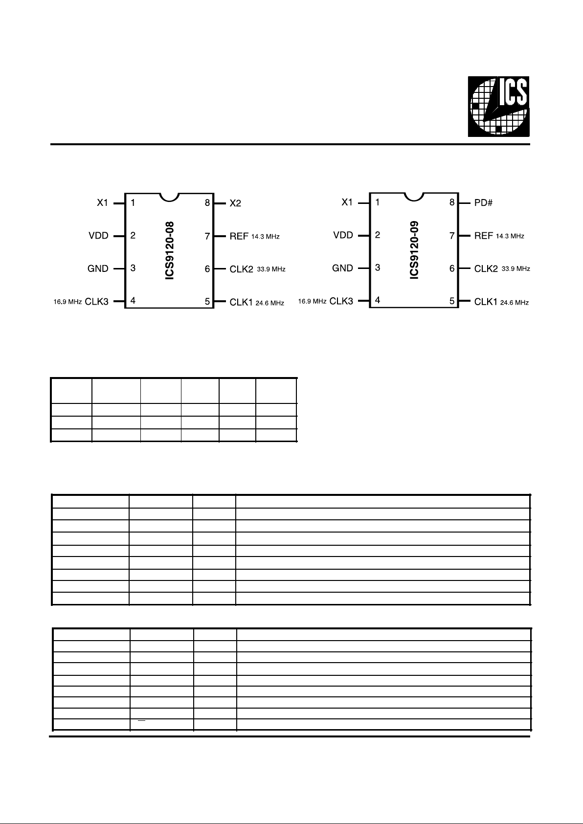
ICS9120-08
ICS9120-09
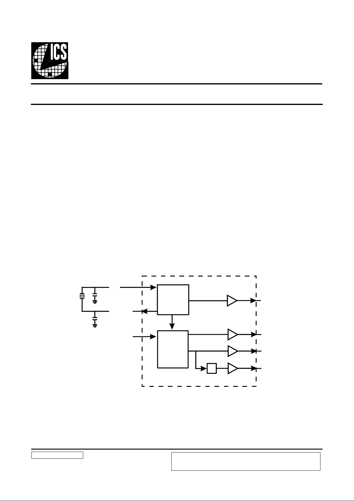
XTAL
OSC
X1
14.318
MHz
X2(-08)
PD(-09)
REF (14.3MHz)
CLK3 (16.9MHz)
CLK2 (33.9MHz)
CLK1 (24.6MHz)
PLL
CLOCK
GEN
External
Crystal
Load Caps
÷2
Frequency Generator for Multimedia Audio Synthesis
9120-08 9120-09 Rev C 052297P
Block Diagram
The ICS9120-08 and ICS 9120-09 are high performance
frequency generators designed to support stereo audio codec
systems. It offers both clock frequencies required by stereo
codecs such as the CS4231 and the AD1848 plus the clock
needed for the OPL4 FM synthesizer. These frequencies can
be synthesized from the existing 14.318 MHz system clock or
from the on-chip oscillator using a 14.318 MHz crystal (-08
only).
High accuracy, low jitter PLLs meet the 0.125% frequency
tolerance and -96dB signal-to-noise ratios required by 16 bit
audio systems. Fast output clock edge rates minimize board
induced jitter.
Unlike competitive devices, the ICS9120-08 and
ICS9120-09 operate over the entire 3.0-5.5V range, with the
-09 providing power-down to minimize energy consumption.
• Generates 16.934 MHz and 24.576 MHz stereo codec
clocks plus the 33.868 MHz OPL4 clock
• Single 14.318MHz crystal or system clock reference
• Buffered REFCLK output
• 0.125% frequency accuracy meets OPL4 specifications
• 100 ps one sigma jitter maintains 16 bit performance
• Output rise/fall times less than 2.0 nS
• On chip loop filter components
• 3.3V - 5 V supply range
• 8 pin, 150mil SOIC package
Applications
• Specifically designed to support the high performance
requirements of multimedia audio systems.
ICS reserves the right to make changes in the device data identified in this publication
without further notice. ICS advises its customers to obtain the latest version of all
device data to verify that any information being relied upon by the customer is current
and accurate.
2
ICS9120-08
ICS9120-09
Pin Configuration
Pin Descriptions for ICS9120-08
Functionality
PIN NUMBER PIN NAME TYPE DESCRIPTION
1 X1 Input Crystal or external clock source. Has feedback bias for crystal.
2V
DD
Power Power supply input.
3 GND Power Ground return for Pin 2.
4 CLK3 Output 16.934 MHz target output clock for stereo codec.
5 CLK1 Output 24.576 MHz target output clock for stereo codec.
6 CLK2 Output 33.868 MHz target output clock for OPL4.
7 REF Output 14.318 MHz reference clock buffered output.
8 X2 Output Crystal output drive.
Pin Descriptions for ICS9120-09
PIN NUMBER PIN NAME TYPE DESCRIPTION
1 X1 Input External clock source.
2 VDD Power Power supply input.
3 GND Power Ground return for Pin 2.
4 CLK3 Output 16.934 MHz target output clock for stereo codec.
5 CLK1 Output 24.576 MHz target output clock for stereo codec.
6 CLK2 Output 33.868 MHz target output clock for OPL4.
7 REF Output 14.318 MHz reference clock buffered output.
8 PD# Input Power-down input powers down entire device when low; has pull-up.
Note: (Pin 8) is internally pulled-up to VDD and, therefore, may
be left disconnected or driven by open collector logic.
8-Pin SOIC
8-Pin SOIC
X1, X2
(MHz)
(-09 only)
PD#
33.9
(MHz)
16.9
(MHz)
24.6
(MHz)
14.3
(MHz)
- 0 Low Low Low Low
14.318 1 33.868 16.934 24.576 14. 318
-
3
ICS9120-08
ICS9120-09
Absolute Maximum Ratings
Electrical Characteristics at 3.3 V
VDD = +3.0 to +3.7 V, TA = 0 to 70oC unless otherwise stated
Note 1: Parameter is guaranteed by design and characterization. Not 100% tested in production.
AVDD, VDD referenced to GND ...................................................................... 7 V
Operating temperature under bias................................................... 0C t o +70C
Storage temperature........................................................................ -65C to +150
Voltage on I/O pins referenced to GND ............... GND -0.5V to VDD +0.5V
Power dissipation ................................................................................... 0.5 Watts
Stresses above those listed under Absolute Maximum Ratings may cause permanent damage to the device. This is a stress
rating only and functional operation of the device at these or any other conditions above those indicated in the operational
sections of the specifications is not implied. Exposure to absolute maximum rating conditions for extended periods may
affect product reliability.
DC Characteristics
PAR AM ET ER SYM BO L TES T C OND IT I ON S MIN TYP MAX UNI TS
Input Low Voltage V
IL
--0.2VDDV
Input High Voltage V
IH
0.7V
DD
--V
Input Low Current I
IL
V
IN
= 0 V (For -09 only) -8.0 -3.6 - µA
Input High Current I
IH
VIN (For -09 only) --5.0µA
Output Low Voltage V
OL
*I
OL
= 6 m A - 0 . 0 5V
DD
0.1 V
Output High Voltage V
OH
*I
OH
= -4.0 mA 0.85V
DD
0.94V
DD
-V
Out p ut Low C ur r e nt I
OL
*V
OL
= 0.2V
DD
15.0 24.0 - mA
Output High Curr ent I
OH
*V
OH
= 0. 7V
DD
--13.0-8.0mA
Supply Current I
CC
Unload ed - 13.0 32.0 mA
Supply Current I
CC(PD)
Unloa d e d ( For -09 only) - 50.0 110. 0 µA
Pull-up Resistor Value R
pu
*(For -09 only) - 620.0 900.0 k ohm

4
ICS9120-08
ICS9120-09
Electrical Characteristics at 3.3 V
VDD = +3.0 to +3.7 V, TA = 0-70oC unless otherwise stated
Note 1: Parameter is guaranteed by design and characterization. Not 100% tested in production.
AC Charact eristics
PARAMETER SYMBOL TEST CONDITIONS MIN TYP MAX UNITS
Rise Time Tr* 15pF load, 0.8 to 2.0V - 1.5 4.0 ns
Fall Time T
f
* 15pF load, 2.0 to 0.8V - 1.0 3.0 ns
Rise Time T
r
* 15pF load, 20% to 80% - 2.2 4.0 ns
Fall Time T
f
* 15pF load, 80% to 20% - 1.5 3.0 ns
Duty Cycle Dt*
15pF load @ 50% of V
DD
;
Except REFCLK
45.0 50.0 55.0 %
Duty Cycle D
t
*
15pF load @ 50% of V
DD
;
REFCLK only
40.0 45.0 60.0 %
Jitter, One Sigma T
jis
*
For all frequencies except
REFCLK
- 150.0 200 ps
Jitter, Absolute T
jab
For all frequencies except
REFCLK
-650.0 380.0 650.0 ps
Jitter, One Sigma T
jis
* REFCLK only - 266.0 400.0 ps
Jitter, Absolute T
jab
REFCLK only -1000 750.0 1000 ps
Input Frequency F
i
* 11.0 14. 3 15.0 MHz
Output Frequency F
o
* 11. 0 - 38. 0 MHz
Output Mean Frequency
Accuracy vs. Target
F
oa*
With 14.318 MHz input -0.125 - -0.04 %
Power-up Time T
pu
* 0 to 33.8 MHz - 5.5 12.0 ms
Crystal Input
Capacitance
C
inx
*
X1 (Pin 1), X2 (Pin 8; -08
only)
-5-pF

5
ICS9120-08
ICS9120-09
Electrical Characteristics at 5.0 V
Note 1: Parameter is guaranteed by design and characterization. Not 100% tested in production.
VDD = +4.5 to +5.5 V, TA = 0-70oC unless otherwise stated
DC Charact eristics
PARAMETER SYMBOL TEST CONDITIONS MIN TYP MAX UNITS
Input Low Voltage V
IL
--0.8V
Input High Voltage V
IH
2.0 - - V
Input Low Current I
IL
V
IN =
0V (For -09 only) -18.0 -8.3 - µA
Input High Current I
IH
VIN = V
DD
(For -09 only)- -5.0µA
Output Low Voltage V
OL
*I
OL
= 10 mA - 0.1 5 0.4 V
Output High Voltage V
OH
*I
OH
= -30 mA 2.4 3.7 - V
Output Low Current I
OL
*V
OL
=0.8V 25.0 45.0 - mA
Output High Current I
OH
*V
OH
= 2. 4V - -53 .0 -35 .0 mA
Supply Current I
CC
Unloaded - 22.0 50.0 mA
Supply Current, Powerdown
I
CC(PD )
Unloaded (For -09 only) - 180.0 500.0 µA
Pull-up Resistor Value R
pu
*(For -09 only) - 400.0 800.0 k ohm

6
ICS9120-08
ICS9120-09
Electrical Characteristics at 5.0 V
VDD = 4.5 - 5.5 V, TA = 0 - 70oC unless otherwise stated
Note 1: Parameter is guaranteed by design and characterization. Not 100% tested in production.
AC Characteristics
PARAMETER
SYMBOL TEST CONDITIONS MIN TYP MAX UNITS
Rise Time Tr* 15pF load, 0.8 to 2.0V - 0.9 2.0 ns
Fall Time T
f
* 15pF load, 2.0 to 0.8V - 0.7 1.5 ns
Rise Time Tr* 15pF load, 20% to 80% - 1.8 3.25 ns
Fall Time T
f
* 15pF load, 80% to 20% - 1.4 2.5 ns
Duty Cycle D
t
*
15pF load @ 50% of V
DD
;
Except REFCLK
45.0 50.0 55.0 %
Duty Cycle D
t
*
15pF load @ 50% of V
DD
;
REFCLK only
40.0 50.0 60.0 %
Jitter, One Sigma T
j1s
*
For all frequencies except
REFCLK
- 100.0 150.0 ps
Jitter, Absolute T
jab
For all frequencies except
REFCLK
-600.0 380.0 600.0 ps
Jitter, One Sigma T
j1s
* REFCLK only - 266.0 450.0 ps
Jitter, Absolute T
jab
REFCLK only -1200 750.0 1200 ps
Input Frequency Range F
i
* 11. 0 14.0 17.0 MHz
Output Frequency
Range
F
o
* 11.0 - 42.0 MHz
Output Mean Frequency
Accuracy vs. Target
Foa* With 14.318 MHz input -0.125 - -0.04 %
Power-up Time T
pu
* 0 to 33 .8 MHz - 5.5 12. 0 ms
Crystal Input
Capacitance
C
inx
* X1 (Pin 1), X2 (Pin 8; -08 only) - 5 - pF

7
ICS9120-08
ICS9120-09
Ordering Information
ICS9120M-08, ICS9120M-09
0.194
0.031
0.024
0.016
0.050
0.006
± 0.004
0.238
0.154
0.015
0.063
0.025
0.008
8-Pin SOIC Package
Example:
ICS XXXX M-PPP
Package Type
M =SOIC
Device Type (consists of 3 or 4-digit numbers)
Prefix
ICS, AV=Standard Device
Pattern Number (2 or 3-digit number for parts with ROM code pattern)
ICS reserves the right to make changes in the device data identified in this publication
without further notice. ICS advises its customers to obtain the latest version of all
device data to verify that any information being relied upon by the customer is current
and accurate.
 Loading...