ICS9112-18
Zero Delay, Low Skew Buffer
Description
The ICS9112-18 is a low jitter, low-skew, high
performance PLL based zero delay buffer for high
speed applications. Based on ICS’s proprietary low
jitter Phase Locked Loop (PLL) techniques, the
device provides eight low skew outputs at speeds
up to 160 MHz at 3.3 V. The ICS9112-18
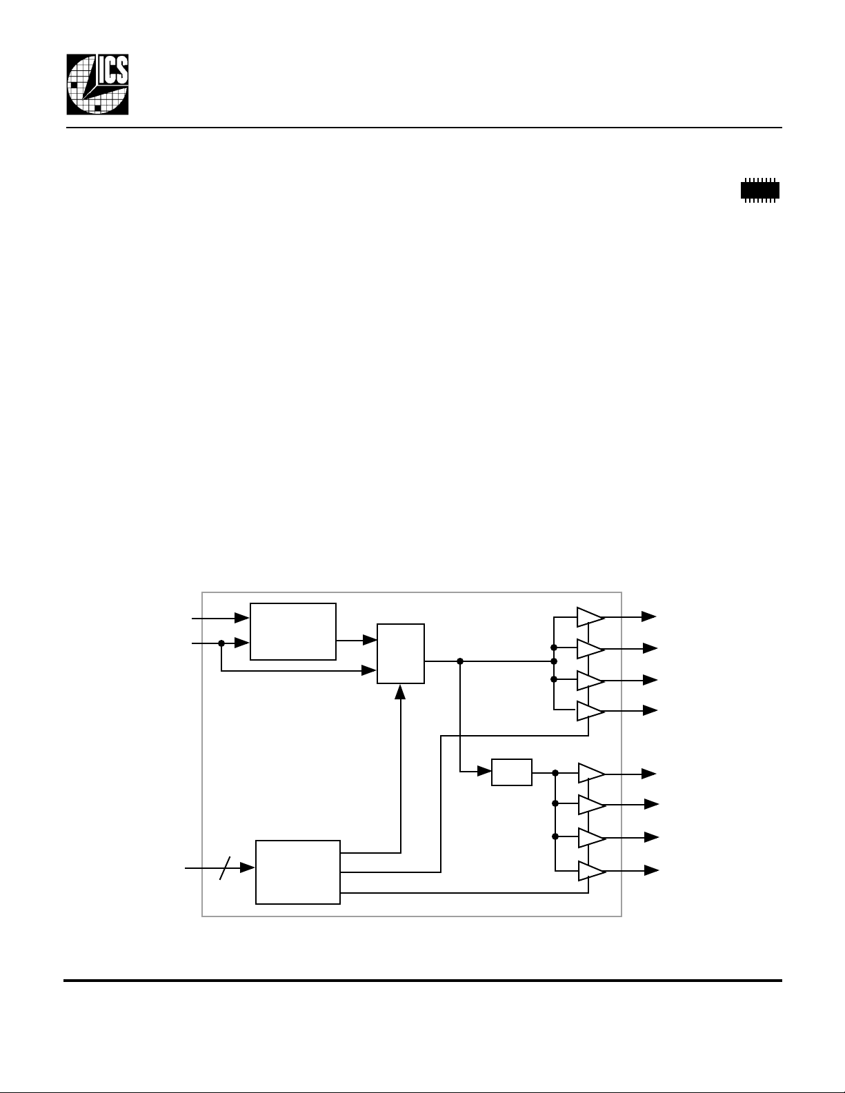
includes a bank of four outputs running at 1X, and
another four outputs running at 1/2X. In the zero
delay mode, the rising edge of the input clock is
aligned with the rising edges of all eight outputs.
Compared to competitive CMOS devices, the
ICS9112-18 has the lowest jitter of all.
ICS manufactures the largest variety of clock
generators and buffers, and is the largest clock
supplier in the world.
Block Diagram
Features
• Packaged in 16 pin narrow SOIC
• Zero input-output delay
• Four 1X outputs plus four half-X outputs
• Output to output skew is less than 250 ps
• Output clocks up to 160 MHz at 3.3 V
• Ability to generate 2X the input
• Full CMOS outputs with 18 mA output drive
capability at TTL levels at 3.3 V
• Spread Smart™ technology works with spread
spectrum clock generators
• Advanced, low power, sub-micron CMOS process
• 3.0 to 5.5 V operating voltage
CLKIN
2
S2, S1
MDS 9112-18 F 1 Revision 050400 Printed 11/15/00
Integrated Circuit Systems, Inc.• 525 Race Street • San Jose • CA • 95126 • (408)295-9800tel• www.icst.com
PLL
Mux
÷ 2
Control
Logic
CLKA1 FBIN
CLKA2
CLKA3
CLKA4
CLKB1
CLKB2
CLKB3
CLKB4

Pin Assignment
ICS9112-18
16
15
14
13
12
11
10
9
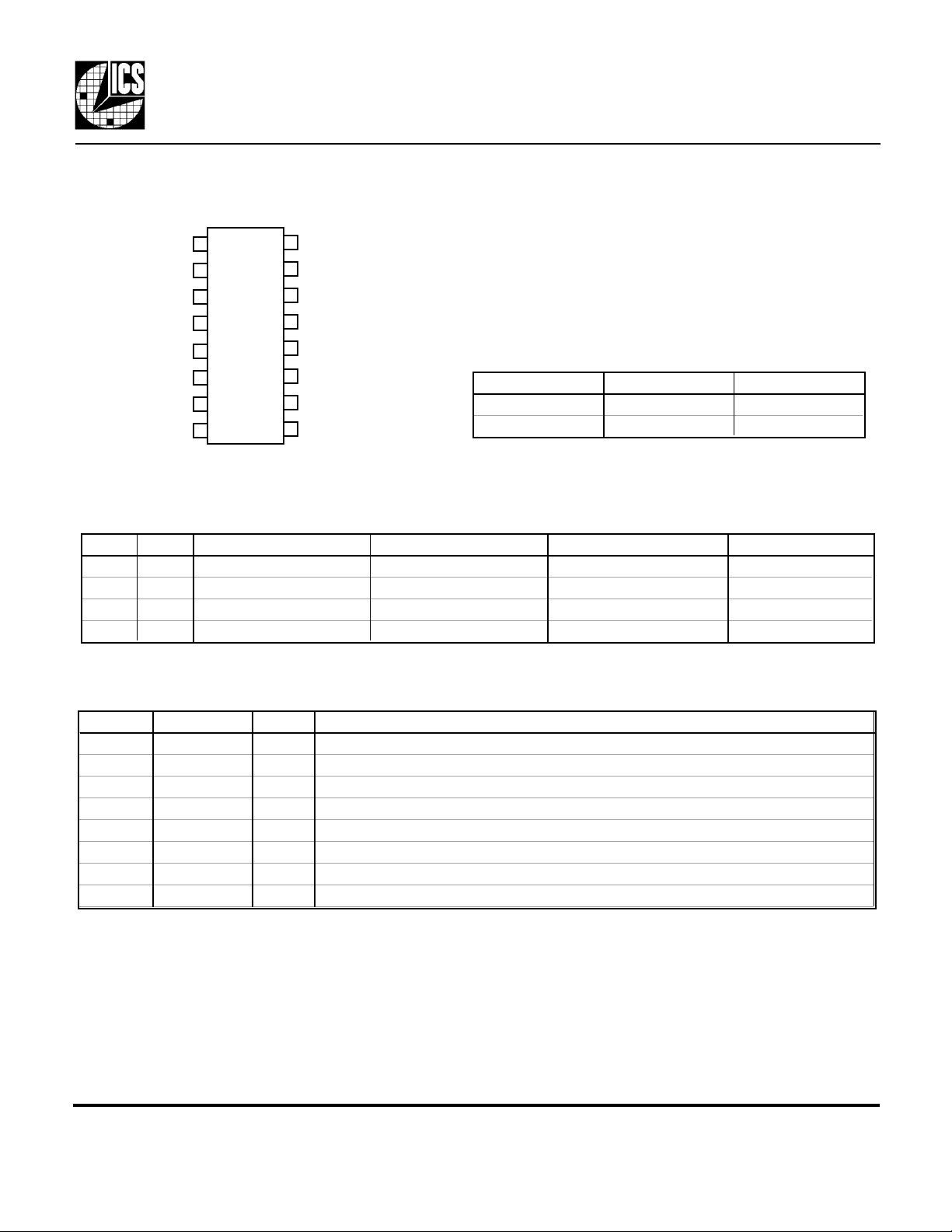
FBIN
CLKA4
CLKA3
VDD
GND
CLKB4
CLKB3
S1
CLKIN
CLKA1
CLKA2
VDD
GND
CLKB1
CLKB2
S2
1
2
3
4
5
6
7
8
16 pin narrow (150 mil) SOIC
Output Clock Mode Select Table
ICS9112-18
Zero Delay, Low Skew Buffer
Feedback Configuration Table
Feedback From CLKA1:A4 CLKB1:B4
Bank A CLKIN CLKIN/2
Bank B 2XCLKIN CLKIN
S2 S1 Clocks A1-A4 Clocks B1-B4 Internal Generation PLL Status
0 0 Tri-state (high impedance) Tri-state (high impedance) None On
0 1 Running Tri-state (high impedance) PLL On
1 0 Running Running Buffer Only (no zero delay) Off
1 1 Running Running PLL On
Pin Descriptions
Number Name Type Description
1 CLKIN I CLocK INput. Connect to input clock source.
2, 3, 14, 15 CLKA1:4 O CLocK A bank of four outputs.
4, 13 VDD P Power supply. Connect both pins to same voltage (either 3.3V or 5V).
5, 12 GND P Connect to ground.
6, 7, 10, 11 CLKB1:4 O CLocK B bank of four outputs. These are low skew divide by two of bank A.
8 S2 I Select input #2. Selects mode for outputs per table above.
9 S1 I Select input #1. Selects mode for outputs per table above.
16 FBIN I FeedBack INput. Determines outputs per Feedback Configuration Table above.
Key: I = Input; O = output; P = power supply connection.
External Components
The ICS9112-18 requires a minimum number of external components for proper operation. Decoupling
capacitors of 0.1µF should be connected between VDD and GND on pins 4 and 5, and VDD and GND
on pins 13 and 12, as close to the device as possible. A series termination resistor of 33 Ω may be used close
to the pin for each clock output to reduce reflections.
MDS 9112-18 F 2 Revision 050400 Printed 11/15/00
Integrated Circuit Systems, Inc.• 525 Race Street • San Jose • CA • 95126 • (408)295-9800tel• www.icst.com
 Loading...