

Integrated
Circuit
Systems, Inc.
ICS8535-01
LOW SKEW, 1-TO-4
LVCMOS-TO-3.3V LVPECL FANOUT BUFFER
GENERAL DESCRIPTION
,&6
HiPerClockS™
the single ended clock input accepts L VCMOS or LVTTL input levels and translate them to 3.3V LVPECL levels. The
clock enable is internally synchronized to eliminate runt clock
pulses on the output during asynchronous assertion/
deassertion of the clock enable pin.
Guaranteed output and part-to-part skew characteristics
make the ICS8535-01 ideal for those applications demanding well defined performance and repeatability.
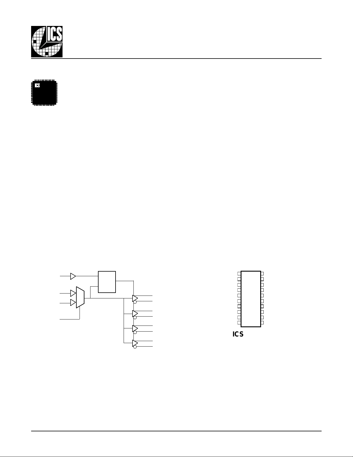
The ICS8535-01 is a low skew, high performance
1-to-4 LVCMOS-to-3.3V LVPECL fanout buffer
and a member of the HiPerClockS™ family of High
Performance Clock Solutions from ICS. The
ICS8535-01 has two single ended clock inputs.
FEATURES
• 4 differential 3.3V L VPECL outputs
• Selectable CLK0 or CLK1 inputs for redundant
and multiple frequency fanout applications
• CLK0 or CLK1 can accept the following differential input
levels: LVCMOS or L VTTL
• Maximum output frequency up to 266MHz
• Translates L VCMOS and LVTTL levels to 3.3V
L VPECL levels
• Output skew: 30ps (maximum)
• Part-to-part skew: 150ps (maximum)
• Propagation delay: 1.9ns (maximum)
• 3.3V operating supply
• 0°C to 70°C ambient operating temperature
• Industrial temperature information available upon request
BLOCK DIAGRAM PIN ASSIGNMENT
CLK_EN
CLK0
CLK1
CLK_SEL
D
Q
LE
0
1
Q0
nQ0
Q1
nQ1
Q2
nQ2
Q3
nQ3
4.4mm x 6.5mm x 0.92mm body package
VEE
CLK_EN
CLK_SEL
CLK0
nc
CLK1
nc
nc
nc
V
CC
ICS8535-01
20-Lead TSSOP
20
1
19
2
18
3
17
4
16
5
15
6
14
7
13
8
12
9
11
10
G Package
T op View
Q0
nQ0
V
CC
Q1
nQ1
Q2
nQ2
V
CC
Q3
nQ3
ICS8535AG-01 www.icst.com/products/hiperclocks.html REV. B JULY 5, 2001
1
Integrated
Circuit
Systems, Inc.
TABLE 1. PIN DESCRIPTIONS
rebmuNemaNepyTnoitpircseD
1V
2NE_KLCtupnIpulluP
3LES_KLCtupnInwodlluP
40KLCtupnInwodlluP.tupnikcolcLTTVL/SOMCVL
61KLCtupnInwodlluP.tupnikcolcLTTVL/SOMCVL
9,8,7,5cndesunU.tcennocoN
81,31,01V
21,113Q,3QntuptuO.slevelecafretniLCEPVL.riaptuptuolaitnereffiD
51,412Q,2QntuptuO.slevelecafretniLCEPVL.riaptuptuolaitnereffiD
71,611Q,1QntuptuO.slevelecafretniLCEPVL.riaptuptuolaitnereffiD
02,910Q,0QntuptuO.slevelecafretniLCEPVL.riaptuptuolaitnereffiD
pulluP
:ETON
EE
CC
dna
nwodlluP
rewoP.dnuorgottcennoC.nipylppusevitageN
rewoP.V3.3ottcecnnoC.snipylppusevitisoP
ICS8535-01
LOW SKEW, 1-TO-4
LVCMOS-TO-3.3V LVPECL FANOUT BUFFER
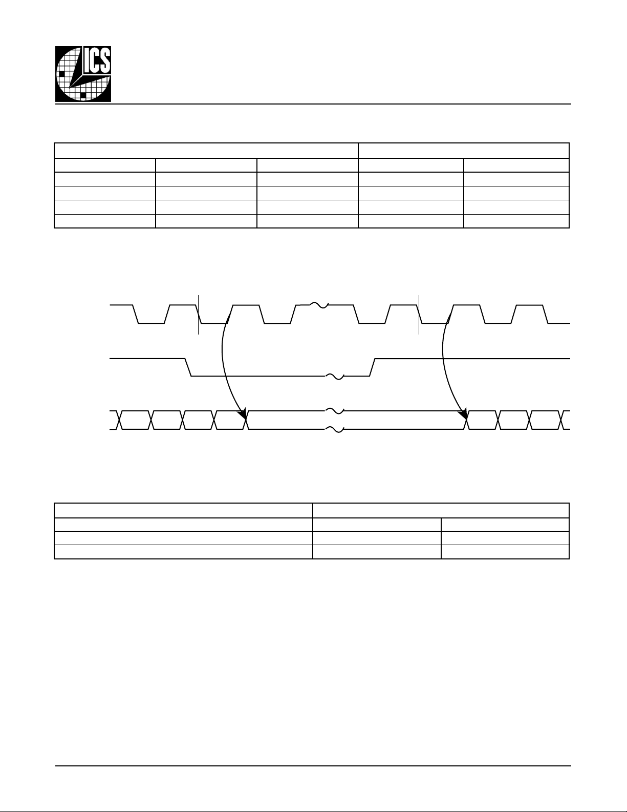
kcolcwollofstuptuokcolc,HGIHnehW.elbanekcolcgnizinorhcnyS
.hgihdecroferastuptuoQn,woldecroferastuptuoQ,WOLnehW.tupni
.slevelecafretniLTTVL/SOMCVL
.tupni1KLCstceles,HGIHnehW.tupnitceleskcolC
.slevelecafretniLTTVL/SOMCVL.tupni0KLCstceles,WOLnehW
.seulavlacipytrof,scitsiretcarahCniP,2elbaTeeS.srotsisertupnilanretniotsrefer
TABLE 2. PIN CHARACTERISTICS
lobmySretemaraPsnoitidnoCtseTmuminiMlacipyTmumixaMstinU
C
NI
R
PULLUP
R
NWODLLUP
1KLC,0KLC4Fp
ecnaticapaCtupnI
rotsiseRpulluPtupnI 15KΩ
,NE_KLC
LES_KLC
rotsiseRnwodlluPtupnI 15KΩ
4Fp
ICS8535AG-01 www.icst.com/products/hiperclocks.html REV. B JULY 5, 2001
2
Integrated
Circuit
Systems, Inc.
TABLE 3A. CONTROL INPUT FUNCTION TABLE
stupnIstuptuO
NE_KLCLES_KLCecruoSdetceleS3Qurht0Q3Qnurht0Qn
00 0KLCWOL;delbasiDHGIH;delbasiD
01 1KLCWOL;delbasiDHGIH;delbasiD
10 0KLCdelbanEdelbanE
11 1KLCdelbanEdelbanE
.1erugiFniwohssa
ICS8535-01
LOW SKEW, 1-TO-4
LVCMOS-TO-3.3V LVPECL FANOUT BUFFER
egdekcolctupnignillafdnagnisiragniwollofdelbanerodelbasiderastuptuokcolceht,sehctiwsNE_KLCretfA
.B3elbaTnidebircsedsastupni1KLCdna0KLCehtfonoitcnufaerastuptuoehtfoetatseht,edomevitcaehtnI
CLK0, CLK1
CLK_EN
nQ0 - nQ3
Q0 - Q3
TABLE 3B. CLOCK INPUT FUNCTION TABLE
stupnIstuptuO
1KLCro0KLC3Qurht0Q3Qnurht0Qn
0WOLHGIH
1HGIHWOL
EnabledDisabled
FIGURE 1 - CLK_EN TIMING DIAGRAM
ICS8535AG-01 www.icst.com/products/hiperclocks.html REV. B JULY 5, 2001
3

Integrated
Circuit
Systems, Inc.
ICS8535-01
LOW SKEW, 1-TO-4
LVCMOS-TO-3.3V LVPECL FANOUT BUFFER
ABSOLUTE MAXIMUM RATINGS
Supply Voltage, V
Inputs, V
I
Outputs, V
Package Thermal Impedance, θ
Storage Temperature, T
CCx
O
JA
STG
Stresses beyond those listed under Absolute Maximum Ratings may cause permanent damage to the device. These ratings are stress specifications only. Functional operation of product at these conditions or any conditions beyond those
listed in the
DC Characteristics
or
AC Characteristics
extended periods may affect product reliability.
4.6V
-0.5V to VCC + 0.5V
-0.5V to VCC + 0.5V
73.2°C/W (no airflow)
-65°C to 150°C
is not implied. Exposure to absolute maximum rating conditions for
TABLE 4A. POWER SUPPLY DC CHARACTERISTICS, V
= 3.3V±5%, TA = 0°C TO 70°C
CC
lobmySretemaraPsnoitidnoCtseTmuminiMlacipyTmumixaMstinU
V
CC
I
EE
egatloVylppuSevitisoP531.33.3564.3V
tnerruCylppuSrewoP 05Am
TABLE 4B. LVCMOS / LVTTL DC CHARACTERISTICS, V
lobmySretemaraPsnoitidnoCtseTmuminiMlacipyTmumixaMstinU
1KLC,0KLC2567.3V
V
HI
V
LI
I
HI
I
LI
egatloVhgiHtupnI
,NE_KLC
LES_KLC
1KLC,0KLC3.0-3.1V
egatloVwoLtupnI
,NE_KLC
LES_KLC
,1KLC,0KLC
tnerruChgiHtupnI
LES_KLC
NE_KLCV
,1KLC,0KLC
tnerruCwoLtupnI
LES_KLC
V
NE_KLCV
= 3.3V±5%, TA = 0°C TO 70°C
CC
V
V=
NI
CC
V=
NI
CC
V,V0=
NI
V,V0=
NI
V564.3=051Aµ
V564.3=5Aµ
CC
CC
V564.3=5-Aµ
V564.3=051-Aµ
2567.3V
3.0-8.0V
TABLE 4C. L VPECL DC CHARACTERISTICS, V
= 3.3V±5%, TA = 0°C TO 70°C
CC
lobmySretemaraPsnoitidnoCtseTmuminiMlacipyTmumixaMstinU
V
HO
V
LO
V
GNIWS
05htiwdetanimretstuptuO:1ETON Ω Vot
ICS8535AG-01 www.icst.com/products/hiperclocks.html REV. B JULY 5, 2001
1ETON;egatloVhgiHtuptuOV
1ETON;egatloVwoLtuptuOV
gniwSegatloVtuptuOkaeP-ot-kaeP6.058.0V
.V2-
CC
4
4.1-V
CC
0.2-V
CC
0.1-V
CC
7.1-V
CC
 Loading...