

Integrated
Circuit
Systems, Inc.
ICS85322
DUAL LVCMOS / LVTTL-TO-DIFFERENTIAL
2.5V / 3.3V LVPECL TRANSLATOR
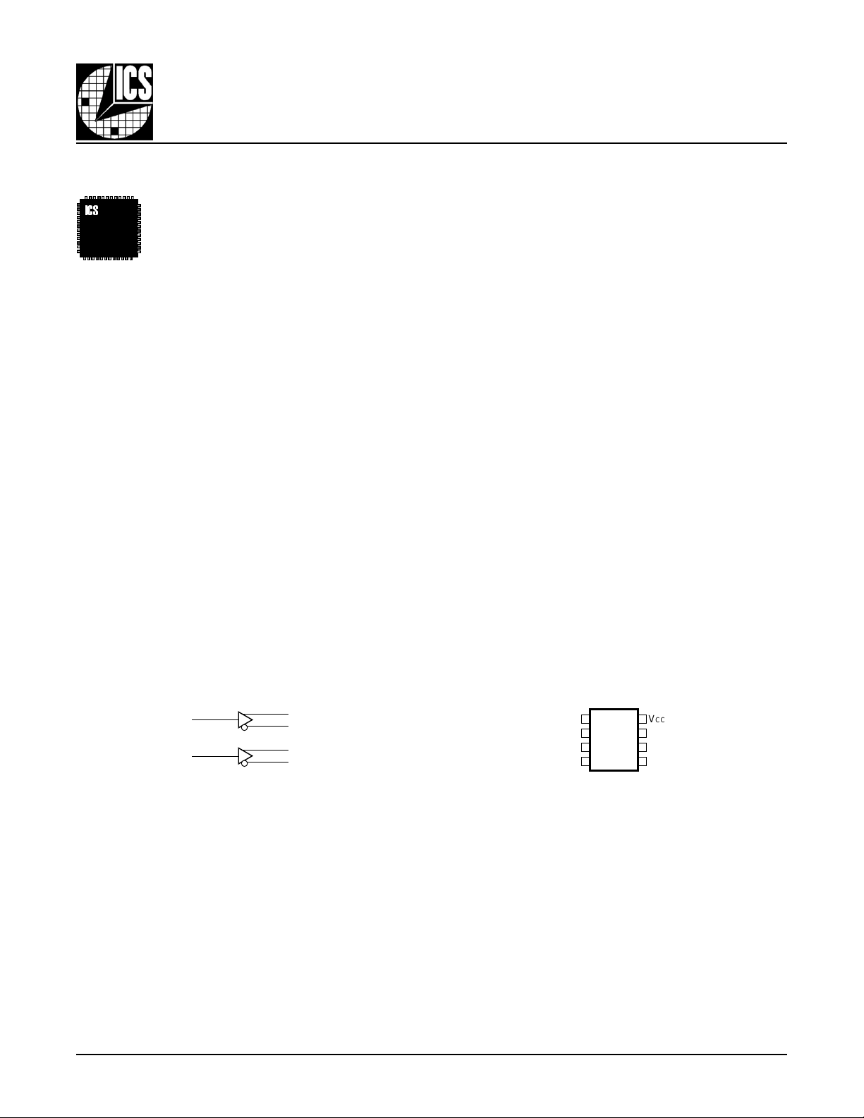
GENERAL DESCRIPTION
,&6
HiPerClockS™
puts. The single ended clock input accepts LVCMOS or LVTTL
input levels and translate them to 2.5V / 3.3V LVPECL levels.
The small outline 8-pin SOIC package makes this device ideal
for applications where space, high performance and low power
are important.
The ICS85322 is a Dual LVCMOS / LVTTL-toDifferential 2.5V / 3.3V L VPECL translator and a
member of the HiPerClocks™ family of High Performance Clocks Solutions from ICS. The
ICS85322 has selectable single ended clock in-
FEATURES
• 2 differential 2.5V/3.3V L VPECL outputs
• Selectable CLK0, CLK1 L VCMOS clock inputs
• CLK0 and CLK1 can accepts the following input levels:
LVCMOS or LVTTL
• Maximum output frequency up to 267MHz
• Part-to-part skew: 150ps (maximum)
• 3.3V operating supply voltage
(operating range 3.135V to 3.465V)
• 2.5V operating supply voltage
(operating range 2.375V to 2.625V)
• 0°C to 70°C ambient operating temperature
• Industrial temperature information available upon request
BLOCK DIAGRAM PIN ASSIGNMENT
CLK0
CLK1
85322AM www.icst.com/products/hiperclocks.html REV. A JULY 31, 2001
Q0
nQ0
Q1
nQ1
Q0
nQ0
Q1
nQ1
1
2
3
4
VCC
8
CLK0
7
6
CLK1
5
V
EE
ICS85322
8-Lead SOIC
3.90mm x 4.92mm x 1.37mm body package
M Package
Top View
1
Integrated
Circuit
Systems, Inc.
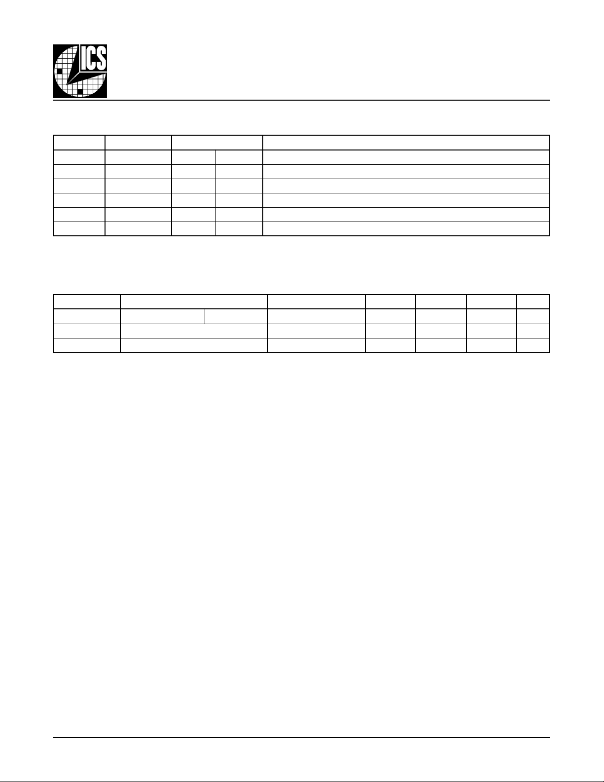
TABLE 1. PIN DESCRIPTIONS
rebmuNemaNepyTnoitpircseD
2,10Qn,0QtuptuO.slevelecafretniLCEPVL.riaptuptuolaitnereffiD
4,31Qn,1QtuptuO.slevelecafretniLCEPVL.riaptuptuolaitnereffiD
5V
61KLCtupnIpulluP.tupnikcolcLTTVL/SOMCVL
70KLCtupnIpulluP.tupnikcolcLTTVL/SOMCVL
8V
pulluP
:ETON
EE
CC
TABLE 2. PIN CHARACTERISTICS
lobmySretemaraPsnoitidnoCtseTmuminiMlacipyTmumixaMstinU
C
NI
R
PULLUP
R
NWODLLUP
rewoP.dnuorgottcennoC.nipylppusevitageN
rewoPV5.2roV3.3ottcennoC.nipylppusevitisoP
ecnaticapaCtupnI1KLC,0KLC4Fp
rotsiseRpulluPtupnI 15KΩ
rotsiseRnwodlluPtupnI 15KΩ
ICS85322
DUAL LVCMOS / LVTTL-TO-DIFFERENTIAL
2.5V / 3.3V LVPECL TRANSLATOR
.seulavlacipytrof,scitsiretcarahCniP,2elbaTeeS.srotsisertupnilanretniotsrefer
85322AM www.icst.com/products/hiperclocks.html REV. A JULY 31, 2001
2
Integrated
Circuit
Systems, Inc.
DUAL LVCMOS / LVTTL-TO-DIFFERENTIAL
ICS85322
2.5V / 3.3V LVPECL TRANSLATOR
ABSOLUTE MAXIMUM RATINGS
Supply Voltage, V
Inputs, V
I
Outputs, V
Package Thermal Impedance, θ
CC
O
JA
Stresses beyond those listed under Absolute Maximum Ratings may cause permanent damage to the device. These ratings
are stress specifications only. Functional operation of product at these conditions or any conditions beyond those listed in
DC Characteristics
the
or
AC Characteristics
periods may affect product reliability .
4.6V
-0.5V to VCC + 0.5V
-0.5V to VCC + 0.5V
112.7°C/W (0lfpm)
is not implied. Exposure to absolute maximum rating conditions for extended
TABLE 3A. POWER SUPPLY DC CHARACTERISTICS, V
= 3.3V±5%, TA = 0°C TO 70°C
CC
lobmySretemaraPsnoitidnoCtseTmuminiMlacipyTmumixaMstinU
V
CC
I
EE
egatloVylppuSevitisoP531.33.3564.3V
tnerruCylppuSrewoP 52Am
TABLE 3B. LVCMOS / LVTTL DC CHARACTERISTICS, V
lobmySretemaraPsnoitidnoCtseTmuminiMlacipyTmumixaMstinU
V
HI
V
LI
I
HI
I
LI
TABLE 3C. LVPECL DC CHARACTERISTICS, V
lobmySretemaraPsnoitidnoCtseTmuminiMlacipyTmumixaMstinU
V
HO
V
LO
V
GNIWS
egatloVhgiHtupnI1KLC,0KLC2567.3V
egatloVwoLtupnI1KLC,0KLC3.0-3.1V
tnerruChgiHtupnI1KLC,0KLCV
tnerruCwoLtupnI1KLC,0KLCV
= 3.3V±5%, TA = 0°C TO 70°C
CC
1ETON;egatloVhgiHtuptuOV
1ETON;egatloVwoLtuptuOV
gniwSegatloVtuptuOkaeP-ot-kaeP56.09.0V
05htiwdetanimretstuptuO:1ETON Ω Vot
.V2-
CC
= 3.3V±5%, TA = 0°C TO 70°C
CC
V=
CC
NI
V=
CC
NI
V=
CC
V=
CC
V564.3=5Aµ
V564.3=051-Aµ
NI
NI
V564.3=V
V564.3=V
4.1-V
CC
0.2-V
CC
0.1-V
CC
7.1-V
CC
85322AM www.icst.com/products/hiperclocks.html REV. A JULY 31, 2001
3
Integrated
Circuit
Systems, Inc.
ICS85322
DUAL LVCMOS / LVTTL-TO-DIFFERENTIAL
2.5V / 3.3V LVPECL TRANSLATOR
TABLE 4A. AC CHARACTERISTICS, V
lobmySretemaraPsnoitidnoCtseTmuminiMlacipyTmumixaMstinU
f
XAM
t
DP
t
)pp(ks3,2ETON;wekStraP-ot-traP 051sp
t
R
t
F
cdoelcyCytuDtuptuO 0406%
emiTesiRtuptuOzHM05@%08ot%02003007sp
emiTllaFtuptuOzHM05@%08ot%02003007sp
= 3.3V±5%, TA = 0°C TO 70°C
CC
ycneuqerFtuptuOmumixaM 762zHM
1ETON;yaleDnoitagaporP ƒ ≤ zHM7626.08.1sn
.stniopssorclaitnereffidehtta
.esiwrehtodetonsselnuzHM331taderusaemsretemarapllA
.tniopgnissorctuptuolaitnereffidehtottupniehtfotniop%05ehtmorfderusaeM:1ETON
segatlovylppusemasehttagnitareposecivedtnereffidnostuptuoneewtebwekssadenifeD:2ETON
derusaemerastuptuoeht,ecivedhcaenostupnifoepytemasehtgnisU.snoitidnocdaollauqehtiwdna
.56dradnatSCEDEJhtiwecnadroccanidenifedsiretemarapsihT:3ETON
85322AM www.icst.com/products/hiperclocks.html REV. A JULY 31, 2001
4

Integrated
Circuit
Systems, Inc.
ICS85322
DUAL LVCMOS / LVTTL-TO-DIFFERENTIAL
2.5V / 3.3V LVPECL TRANSLATOR
TABLE 3D. POWER SUPPLY DC CHARACTERISTICS, V
= 2.5V±5%, TA = 0°C TO 70°C
CC
lobmySretemaraPsnoitidnoCtseTmuminiMlacipyTmumixaMstinU
V
CC
I
EE
egatloVylppuSevitisoP573.25.2526.2V
tnerruCylppuSrewoP 52Am
TABLE 3E. LVCMOS / LVTTL DC CHARACTERISTICS, V
lobmySretemaraPsnoitidnoCtseTmuminiMlacipyTmumixaMstinU
V
HI
V
LI
I
HI
I
LI
TABLE 3F. LVPECL DC CHARACTERISTICS, V
lobmySretemaraPsnoitidnoCtseTmuminiMlacipyTmumixaMstinU
V
HO
V
LO
V
GNIWS
egatloVhgiHtupnI1KLC,0KLC6.1529.2V
egatloVwoLtupnI1KLC,0KLC3.0-9.0V
tnerruChgiHtupnI1KLC,0KLCV
tnerruCwoLtupnI1KLC,0KLCV
= 2.5V±5%, TA = 0°C TO 70°C
CC
1ETON;egatloVhgiHtuptuOV
1ETON;egatloVwoLtuptuOV
gniwSegatloVtuptuOkaeP-ot-kaeP56.09.0V
05htiwdetanimretstuptuO:1ETON Ω Vot
.V2-
CC
= 2.5V±5%, TA = 0°C TO 70°C
CC
V=
CC
NI
V=
CC
NI
526.2=5Aµ
526.2=051-Aµ
CC
CC
4.1-V
0.2-V
0.1-V
CC
7.1-V
CC
TABLE 4B. AC CHARACTERISTICS, V
= 2.5V±5%, TA = 0°C TO 70°C
CC
lobmySretemaraPsnoitidnoCtseTmuminiMlacipyTmumixaMstinU
f
XAM
t
DP
t
)pp(ks3,2ETON;wekStraP-ot-traP 051sp
t
R
t
F
emiTesiRtuptuOzHM05@%08ot%02003007sp
emiTllaFtuptuOzHM05@%08ot%02003007sp
ycneuqerFtuptuOmumixaM 512zHM
1ETON;yaleDnoitagaporP ƒ ≤ zHM5128.02sn
cdoelcyCytuDtuptuO 0406%
.esiwrehtodetonsselnuzHM331taderusaemsretemarapllA
.tniopgnissorctuptuolaitnereffidehtottupniehtfotniop%05ehtmorfderusaeM:1ETON
segatlovylppusemasehttagnitareposecivedtnereffidnostuptuoneewtebwekssadenifeD:2ETON
derusaemerastuptuoeht,ecivedhcaenostupnifoepytemasehtgnisU.snoitidnocdaollauqehtiwdna
.stniopssorclaitnereffidehtta
..56dradnatSCEDEJhtiwecnadroccanidenifedsiretemarapsihT:3ETON
85322AM www.icst.com/products/hiperclocks.html REV. A JULY 31, 2001
5
Integrated
Circuit
Systems, Inc.
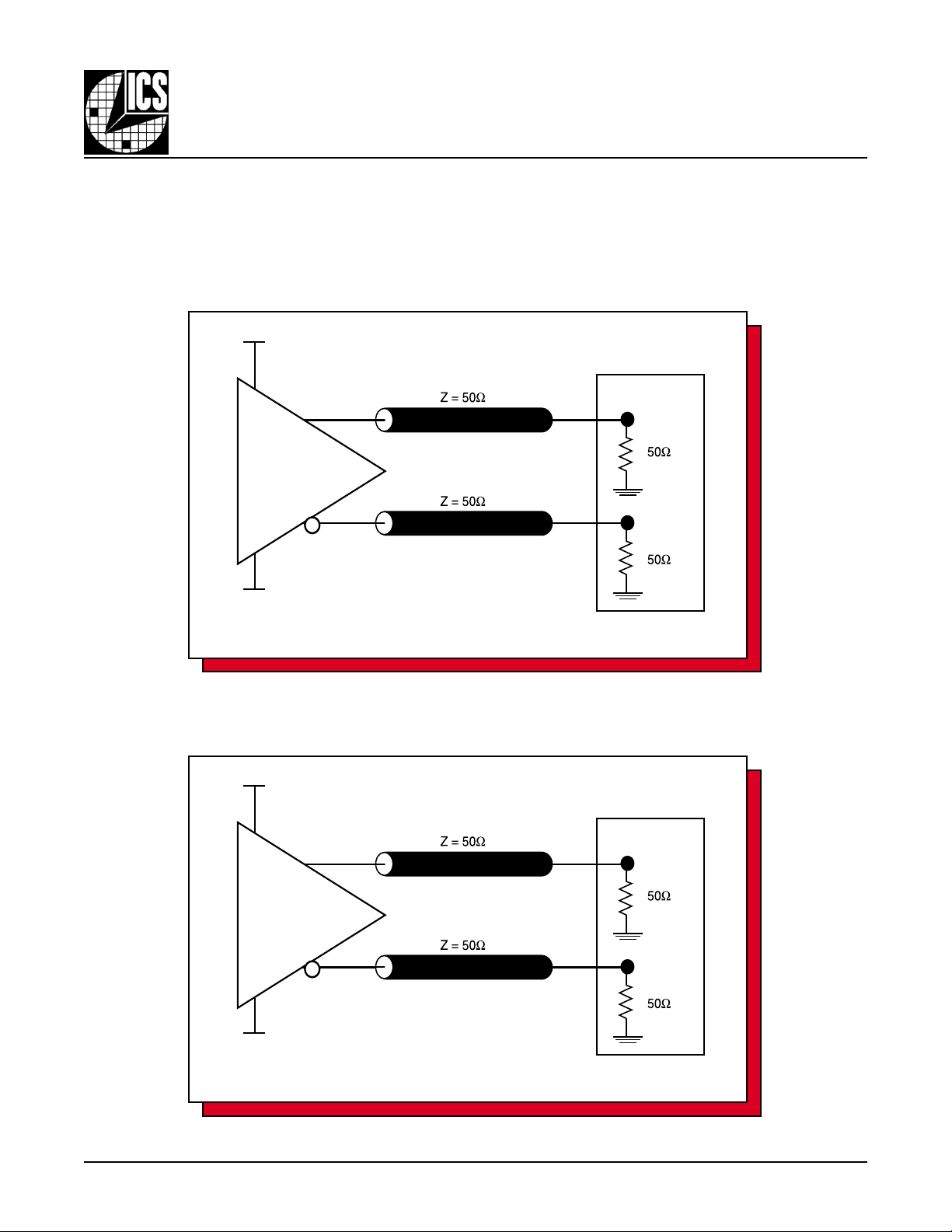
PARAMETER MEASUREMENT INFORMATION
V
CC
LVPECL
VCC = 2V
ICS85322
DUAL LVCMOS / LVTTL-TO-DIFFERENTIAL
2.5V / 3.3V LVPECL TRANSLATOR
SCOPE
Qx
nQx
VEE = -1.3V ± 0.135V
FIGURE 1A - 3.3V OUTPUT LOAD TEST CIRCUIT
V
CC
LVPECL
VCC = 2V
VEE = -0.5V ± 0.125V
SCOPE
Qx
nQx
FIGURE 1B - 2.5V OUTPUT LOAD TEST CIRCUIT
85322AM www.icst.com/products/hiperclocks.html REV. A JULY 31, 2001
6
Integrated
Circuit
Systems, Inc.
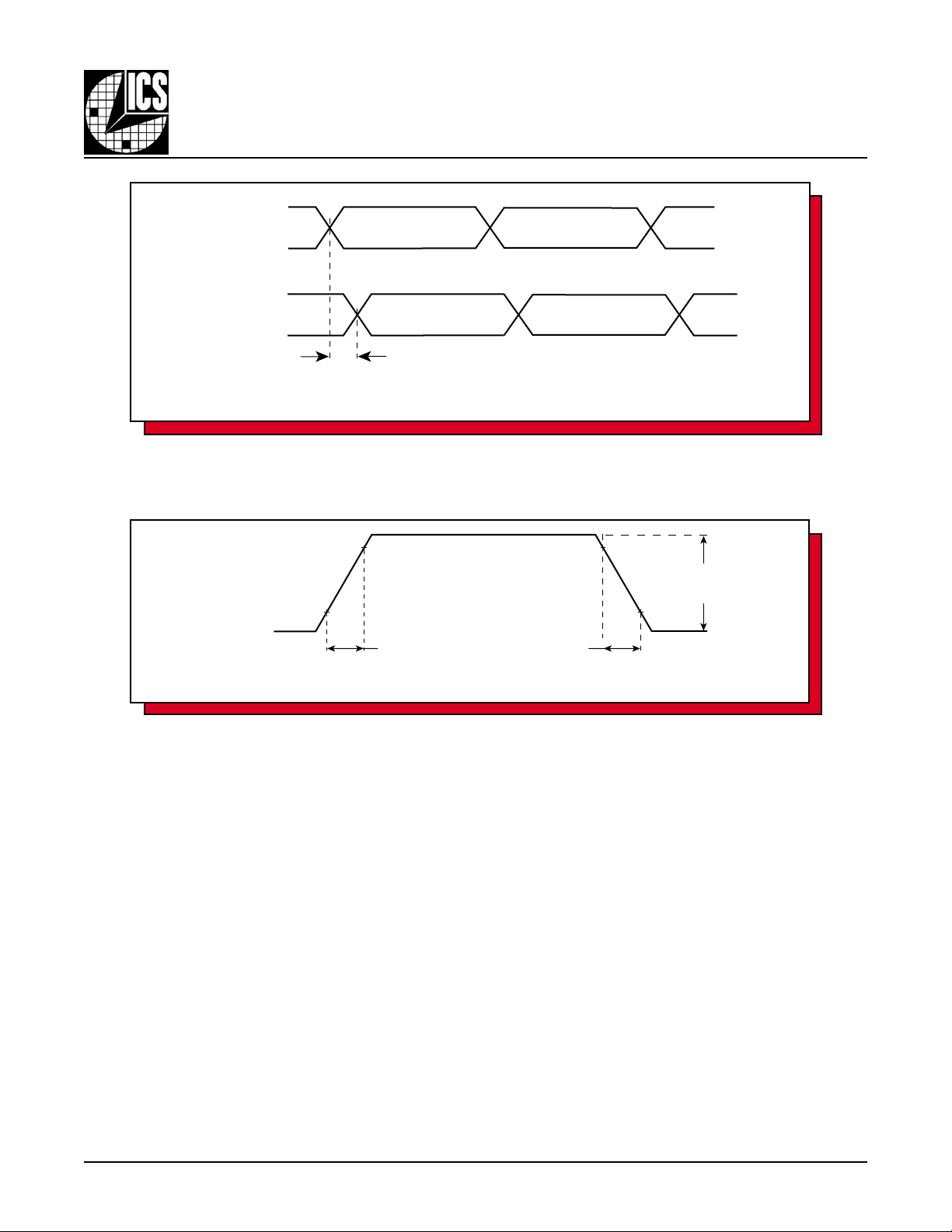
Qx
PART 1
nQx
Qy
PART 2
nQy
ICS85322
DUAL LVCMOS / LVTTL-TO-DIFFERENTIAL
2.5V / 3.3V LVPECL TRANSLATOR
tsk(pp)
FIGURE 2 - PART-TO-PART SKEW
Clock Inputs
and Outputs
80%
20%
t
R
t
F
FIGURE 3 - INPUT AND OUTPUT RISE AND FALL TIME
80%
20%
V
SWING
85322AM www.icst.com/products/hiperclocks.html REV. A JULY 31, 2001
7

Integrated
Circuit
Systems, Inc.
CLK0, CLK1
Q0 - Q1
nQ0 - nQ1
CLK0, CLK1, Q0, Q1
DUAL LVCMOS / LVTTL-TO-DIFFERENTIAL
VCC/2
t
PD
FIGURE 4 - PROPAGATION DELAY
ICS85322
2.5V / 3.3V LVPECL TRANSLATOR
nQ0, nQ1
Pulse Width
t
t
PERIOD
PW
odc =
FIGURE 5 - odc & t
t
PERIOD
PERIOD
85322AM www.icst.com/products/hiperclocks.html REV. A JULY 31, 2001
8

Integrated
Circuit
Systems, Inc.
DUAL LVCMOS / LVTTL-TO-DIFFERENTIAL
ICS85322
2.5V / 3.3V LVPECL TRANSLATOR
POWER CONSIDERA TIONS
This section provides information on power dissipation and junction temperature for the ICS85322.
Equations and example calculations are also provided.
1. Power Dissipation.
The total power dissipation for the ICS85322 is the sum of the core power plus the power dissipated in the load(s).
The following is the power dissipation for V
NOTE: Please refer to Section 3 for details on calculating power dissipated in the load.
= 3.3V + 5% = 3.465V , which gives worst case results.
CC
• Power (core)
• Power (outputs)
If all outputs are loaded, the total power is 2 * 30.2mW = 60.4mW
T otal Power
MAX
= V
MAX
_MAX
* I
CC_MAX
= 30.2mW/Loaded Output pair
= 3.465V * 25mA = 86.6mW
EE_MAX
(3.465V , with all outputs switching) = 86.6mW + 60.4mW = 147mW
2. Junction T emperature.
Junction temperature, Tj, is the temperature at the junction of the bond wire and bond pad and directly affects the reliability of the
device. The maximum recommended junction temperature for HiPerClockS
The equation for Tj is as follows: Tj = θ
Tj = Junction T emperature
θ
= junction-to-ambient thermal resistance
JA
Pd_total = T otal device power dissipation (example calculation is in section 1 above)
T
= Ambient T emperature
A
In order to calculate junction temperature, the appropriate junction-to-ambient thermal resistance θ
moderate air flow of 200 linear feet per minute and a multi-layer board, the appropriate value is 103.3°C/W per Table 5 below.
Therefore, Tj for an ambient temperature of 70°C with all outputs switching is:
70°C + 0.147W * 103.3°C/W = 85.2°C. This is well below the limit of 125°C
This calculation is only an example. Tj will obviously vary depending on the number of loaded outputs, supply voltage, air flow,
and the type of board (single layer or multi-layer).
* Pd_total + T
JA
A
TM
devices is 125°C.
must be used . Assuming a
JA
Table 5. Thermal Resistance qJA for 8-pin SOIC, Forced Convection
q
by V elocity (Linear Feet per Minute)
JA
0 200 500
Single-Layer PCB, JEDEC Standard Test Boards 153.3°C/W 128.5°C/W 115.5°C/W
Multi-Layer PCB, JEDEC Standard Test Boards 112.7°C/W 103.3°C/W 97.1°C/W
NOTE: Most modern PCB designs use multi-layered boards. The data in the second row pertains to most designs.
85322AM www.icst.com/products/hiperclocks.html REV. A JULY 31, 2001
9
Integrated
Circuit
Systems, Inc.
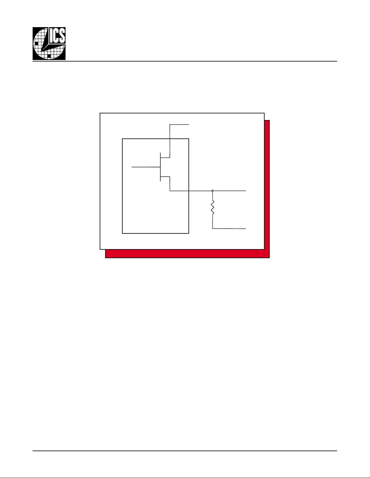
3. Calculations and Equations.
The purpose of this section is to derive the power dissipated into the load.
DUAL LVCMOS / LVTTL-TO-DIFFERENTIAL
ICS85322
2.5V / 3.3V LVPECL TRANSLATOR
LVPECL output driver circuit and termination are shown in
Figure 6.
VCC
Q1
V
OUT
RL
50
V
- 2V
CC
FIGURE 6 - LVPECL DRIVER CIRCUIT AND TERMINATION
To calculate worst case power dissipation into the load, use the following equations which assume a 50Ω load, and a termination
voltage of V
Pd_H is power dissipation when the output drives high.
Pd_L is the power dissipation when the output drives low .
CC
- 2V .
Pd_H = [(V
Pd_L = [(V
• For logic high, V
Using V
• For logic low, V
Using V
OH_MAX
OL_MAX
– (V
– (V
CC_MAX
CC_MAX
- 2V))/RL] * (V
CC_MAX
- 2V))/RL] * (V
CC_MAX
= V
OUT
OH_MAX
= 3.465, this results in V
= V
OUT
OL_MAX
= 3.465, this results in V
= V
= V
CC_MAX
CC_MAX
CC_MAX
CC_MAX
- V
OH_MAX
- V
OL_MAX
– 1.0V
OH_MAX
– 1.7V
OL_MAX
)
)
= 2.465V
= 1.765V
Pd_H = [(2.465V - (3.465V - 2V))/50Ω] * (3.465V - 2.465V) = 20mW
Pd_L = [(1.765V - (3.465V - 2V))/50Ω] * (3.465V - 1.765V) = 10.2mW
T otal Power Dissipation per output pair = Pd_H + Pd_L = 30.2mW
85322AM www.icst.com/products/hiperclocks.html REV. A JULY 31, 2001
10

Integrated
Circuit
Systems, Inc.
ICS85322
DUAL LVCMOS / LVTTL-TO-DIFFERENTIAL
2.5V / 3.3V LVPECL TRANSLATOR
RELIABILITY INFORMATION
TABLE 6. θ
TRANSISTOR COUNT
The transistor count for ICS85322 is: 269
VS
. AIR FLOW TABLE
JA
Single-Layer PCB, JEDEC Standard Test Boards 153.3°C/W 128.5°C/W 115.5°C/W
Multi-Layer PCB, JEDEC Standard Test Boards 112.7°C/W 103.3°C/W 97.1°C/W
NOTE: Most modern PCB designs use multi-layered boards. The data in the second row pertains to most designs.
q
by V elocity (Linear Feet per Minute)
JA
0 200 500
85322AM www.icst.com/products/hiperclocks.html REV. A JULY 31, 2001
11
Integrated
Circuit
Systems, Inc.
PACKAGE OUTLINE - M SUFFIX
ICS85322
DUAL LVCMOS / LVTTL-TO-DIFFERENTIAL
2.5V / 3.3V LVPECL TRANSLATOR
TABLE 7. PACKAGE DIMENSIONS
LOBMYS
N8
A53.157.1
1A01.052.0
B33.015.0
C91.052.0
D08.400.5
E08.300.4
eCISAB72.1
H08.502.6
h52.005.0
L04.072.1
α
Reference Document: JEDEC Publication 95, MS-012
85322AM www.icst.com/products/hiperclocks.html REV. A JULY 31, 2001
NUMINIMMUMIXAM
°0 °8
12
sretemilliM

Integrated
Circuit
Systems, Inc.
TABLE 8. ORDERING INFORMATION
rebmuNredrO/traPgnikraMegakcaPtnuoCerutarepmeT
MA22358SCIMA22358SCICIOSdael8ebutrep69C°07otC°0
T-MA22358SCIMA223358SCIleeRdnaepaTnoCIOSdael80052C°07otC°0
ICS85322
DUAL LVCMOS / LVTTL-TO-DIFFERENTIAL
2.5V / 3.3V LVPECL TRANSLATOR
While the information presented herein has been checked for both accuracy and reliability, Integrated Circuit Systems, Incorporated (ICS) assumes no responsibility for either its use
or for infringement of any patents or other rights of third parties, which would result from its use. No other circuits, patents, or licenses are implied. This product is intended for use
in normal commercial applications. Any other applications such as those requiring extended temperature range, high reliability, or other extraordinary environmental requirements are
not recommended without additional processing by ICS. ICS reserves the right to change any circuitry or specifications without notice. ICS does not authorize or warrant any ICS
product for use in life support devices or critical medical instruments.
85322AM www.icst.com/products/hiperclocks.html REV. A JULY 31, 2001
13
 Loading...