

Integrated
Circuit
Systems, Inc.
ICS8531-01
LOW SKEW, 1-TO-9
DIFFERENTIAL-TO-3.3V LVPECL FANOUT BUFFER
GENERAL DESCRIPTION
,&6
HiPerClockS™
inputs. The CLK, nCLK pair can accept most standard
differential input levels. The PCLK, nPCLK pair can accept
LVPECL, CML, or SSTL input levels. The clock enable is
internally synchronized to eliminate runt pulses on the outputs during asynchronous assertion/deassertion of the clock
enable pin.
Guaranteed output skew and part-to-part skew characteristics make the ICS8531-01 ideal for high performance workstation and server applications.
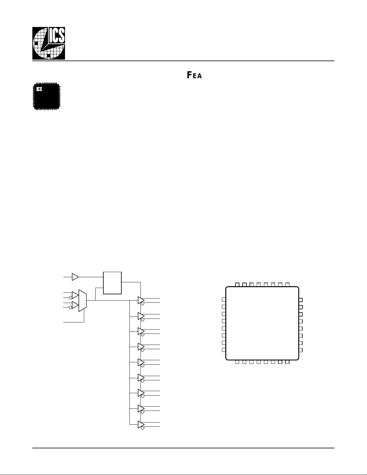
The ICS8531-01 is a low skew , high performance
1-to-9 Differential-to-3.3V L VPECL Fanout Buffer
and a member of the HiPerClockS™
family of High Performance Clock Solutions from
ICS. The ICS8531-01 has two selectable clock
FEATURES
• 9 differential 3.3V L VPECL outputs
• Selectable CLK, nCLK or L VPECL clock inputs
• CLK, nCLK pair can accept the following differential input
levels: L VDS, L VPECL, L VHSTL, SSTL, HCSL
• PCLK, nPCLK supports the following input types:
LVPECL, CML, SSTL
• Maximum output frequency up to 500MHz
• Translates any single ended input signal (L VCMOS, L VTTL,
GTL) to 3.3V L VPECL levels with resistor bias on nCLK input
• Output skew: 50ps (maximum)
• Part-to-part skew: 250ps (maximum)
• Propagation delay: 2ns (maximum)
• 3.3V operating supply
• 0°C to 70°C ambient operating temperature
• Industrial temperature information available upon request
BLOCK DIAGRAM PIN ASSIGNMENT
V
CCO
CLK_EN
CLK
nCLK
PCLK
nPCLK
CLK_SEL
D
Q
LE
0
1
Q0
nQ0
Q1
nQ1
Q2
nQ2
Q3
nQ3
Q4
nQ4
Q5
nQ5
Q6
nQ6
Q7
nQ7
Q8
nQ8
VCC
CLK
nCLK
CLK_SEL
PCLK
nPCLK
EE
V
CLK_EN
7mm x 7mm x 1.4mm package body
Q0
32 31 30 29 28 27 26 25
1
2
3
4
ICS8531-01
5
6
7
8
9 10 11 12 13 14 15 16
nQ8
Vcco
32-Lead LQFP
nQ1
nQ0
Q1
Q7
nQ7
Q8
Y package
Top View
Q2
nQ6
nQ2
Q6
VCCO
Vcco
24
23
22
21
20
19
18
17
CCO
V
Q3
nQ3
Q4
nQ4
Q5
nQ5
CCO
V
8531AY-01 www.icst.com/products/hiperclocks.html REV. B AUGUST 9, 2001
1
Integrated
Circuit
Systems, Inc.
TABLE 1. PIN DESCRIPTIONS
rebmuNemaNepyTnoitpircseD
1V
2KLCtupnInwodlluP.tupnikcolclaitnereffidgnitrevni-noN
3KLCntupnIpulluP.tupnikcolclaitnereffidgnitrevnI
4LES_KLCtupnInwodlluP
5KLCPtupnInwodlluP.tupnikcolcLCEPVLlaitnereffidgnitrevni-noN
6KLCPntupnIpulluP.tupnikcolcLCEPVLlaitnereffidgnitrevnI
7V
8NE_KLCtupnIpulluP
,71,61,9
23,52,42
11,018Q,8QntuptuO.levelecafretniLCEPVL.riaptuptuolaitnereffiD
31,217Q,7QntuptuO.levelecafretniLCEPVL.riaptuptuolaitnereffiD
51,416Q,6QntuptuO.levelecafretniLCEPVL.riaptuptuolaitnereffiD
91,815Q,5QntuptuO.levelecafretniLCEPVL.riaptuptuolaitnereffiD
12,024Q,4QntuptuO.levelecafretniLCEPVL.riaptuptuolaitnereffiD
32,223Q3QntuptuO.levelecafretniLCEPVL.riaptuptuolaitnereffiD
72,622Q,2QntuptuO.levelecafretniLCEPVL.riaptuptuolaitnereffiD
92,821Q,1QntuptuO.levelecafretniLCEPVL.riaptuptuolaitnereffiD
13,030Q,0QntuptuO.levelecafretniLCEPVL.riaptuptuolaitnereffiD
:ETON
pulluP
CC
EE
V
OCC
dna
nwodlluP
rewoP.V3.3ottcennoC.nipylppusevitisoP
rewoP.dnuorgottcennoC.nipylppusevitageN
rewoP.V3.3ottcennoC.snipylppustuptuO
ICS8531-01
LOW SKEW, 1-TO-9
DIFFERENTIAL-TO-3.3V LVPECL FANOUT BUFFER
.stupniKLCPn,KLCPstceles,HGIHnehW.tupnitceleSkcolC
stceles,WOLnehW.KLCn,KLC
.slevelecafretniSOMCVL/LTTVL
wollofstuptuokcolc,HGIHnehW.elbanekcolcgnizinorhcnyS
stuptuoQn,woldecroferastuptuoQ,WOLnehW.tupnikcolc
.slevelecafretniSOMCVL/LTTVL.hgihdecrofera
.seulavlacipytrof,scitsiretcarahCniP,2elbaTeeS.srotsisertupnilanretniotsrefer
TABLE 2. PIN CHARACTERISTICS
lobmySretemaraPsnoitidnoCtseTmuminiMlacipyTmumixaMstinU
,KLCn,KLC
C
NI
R
PULLUP
R
8531AY-01 www.icst.com/products/hiperclocks.html REV. B AUGUST 9, 2001
NWODLLUP
ecnaticapaCtupnI
rotsiseRpulluPtupnI 15KΩ
rotsiseRnwodlluPtupnI 15KΩ
KCLPn,KLCP
LES_KLC,NE_KLC4Fp
2
4Fp
Integrated
Circuit
Systems, Inc.
TABLE 3A. CONTROL INPUT FUNCTION TABLE
stupnIstuptuO
NE_KLCLES_KLCdecruoSdetceleS8Qurht0Q8Qnurht0Qn
00 KLCn,KLCWOL;delbasiDHGIH;delbasiD
01 KLCPn,KLCPWOL;delbasiDHGIH;delbasiD
10 KLCn,KLCdelbanEdelbanE
11 KLCPn,KLCPdelbanEdelbanE
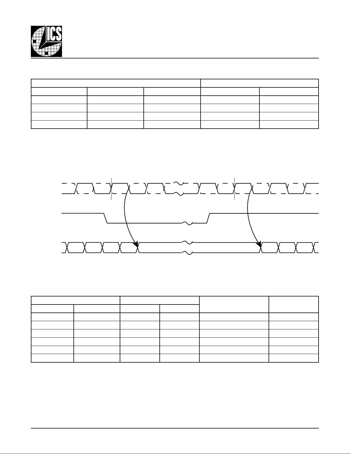
.1erugiFninwohssa
.B3elbaTni
ICS8531-01
LOW SKEW, 1-TO-9
DIFFERENTIAL-TO-3.3V LVPECL FANOUT BUFFER
egdekcolctupnignillafdnagnisiragniwollofdelbanerodelbasiderastuptuokcolceht,sehctiwsNE_KLCretfA
debircsedsastupniKLCPn,KLCPdnaKLCn,KLCehtfonoitcnufaerastuptuoehtfoetatseht,edomevitcaehtnI
nCLK, nPCLK
CLK, PCLK
CLK_EN
nQ0 - nQ8
Q0 - Q8
Disabled
TABLE 3B. CLOCK INPUTS FUNCTION TABLE
stupnIstuptuO
KLCProKLCKLCPnroKLCn8Qurht0Q8Qnurht0Qn
01WOLHGIHlaitnereffiDotlaitnereffiDgnitrevnInoN
10 HGIHWOLlaitnereffiDotlaitnereffiDgnitrevnInoN
01ETON;desaiBWOLHGIHlaitnereffiDotdednEelgniSgnitrevnInoN
11ETON;desaiBHGIHWOLlaitnereffiDotdednEelgniSgnitrevnInoN
1ETON;desaiB0HGIHWOLlaitnereffiDotdednEelgniSgnitrevnI
1ETON;desaiB1WOLHGIHlaitnereffiDotdednEelgniSgnitrevnI
.sleveldedneelgnistpeccaottupni
Enabled
FIGURE 1: CLK_EN TIMING DIAGRAM
edoMtuptuOottupnIytiraloP
laitnereffidehtgniriwsessucsidhcihw,9erugiF,8egapnonoitcesnoitamrofnInoitacilppAehtotreferesaelP:1ETON
8531AY-01 www.icst.com/products/hiperclocks.html REV. B AUGUST 9, 2001
3
Integrated
Circuit
Systems, Inc.
ICS8531-01
LOW SKEW, 1-TO-9
DIFFERENTIAL-TO-3.3V LVPECL FANOUT BUFFER
ABSOLUTE MAXIMUM RATINGS
Supply Voltage, V
Inputs, V
I
Outputs, V
Package Thermal Impedance, θ
Storage T emperature, T
CCx
O
JA
STG
Stresses beyond those listed under Absolute Maximum Ratings may cause permanent damage to the device. These ratings
are stress specifications only. Functional operation of product at these conditions or any conditions beyond those listed in the
DC Characteristics
or
AC Characteristics
ods may affect product reliability .
4.6V
-0.5V to VCC + 0.5V
-0.5V to V
CCO
+ 0.5V
47.9°C/W
-65°C to 150°C
is not implied. Exposure to absolute maximum rating conditions for extended peri-
TABLE 4A. POWER SUPPLY DC CHARACTERISTICS, V
lobmySretemaraPsnoitidnoCtseTmuminiMlacipyTmumixaMstinU
V
CC
V
OCC
I
EE
TABLE 4B. LVCMOS DC CHARACTERISTICS, V
egatloVylppuSevitisoP 531.33.3564.3V
egatloVylppuStuptuO 531.33.3564.3V
tnerruCylppuSrewoP 0507Am
= V
CC
lobmySretemaraPsnoitidnoCtseTmuminiMlacipyTmumixaMstinU
V
HI
V
LI
I
HI
I
LI
LES_KLC,NE_KLC2567.3V
LES_KLC,NE_KLC3.0-8.0V
tnerruChgiHtupnI
tnerruCwoLtupnI
NE_KLCV
LES_KLCV
NE_KLCV
LES_KLCV
TABLE 4C. DIFFERENTIAL DC CHARACTERISTICS, V
lobmySretemaraPsnoitidnoCtseTmuminiMlacipyTmumixaMstinU
KLCV
I
HI
I
LI
V
PP
V
RMC
2,1ETON
tnerruChgiHtupnI
tnerruCwoLtupnI
KLCnV
KLCV
KLCnV
egatloVtupnIkaeP-ot-kaeP51.03.1V
;egatloVtupnIedoMnommoC
= V
= 3.3V±5%, TA = 0°C TO 70°C
CCO
= 3.3V±5%, TA = 0°C TO 70°C
V=
CC
NI
V=
CC
NI
V,V0=
NI
NI
CCO
V=
V=
V,V0=
V,V0=
VsadenifedsiegatlovtupniedomnommoC:2ETON
.
CC
V,V0=
CC
= 3.3V±5%, TA = 0°C TO 70°C
NI
NI
V564.3=051Aµ
V564.3=5Aµ
CC
CC
V564.3=5-Aµ
V564.3=051-Aµ
CC
NI
NI
CC
CCO
= V
CC
CC
V564.3=5Aµ
V564.3=051Aµ
V564.3=051-Aµ
V564.3=5-Aµ
V
5.0+V
EE
VsiKLCndnaKLCrofegatlovtupnimumixameht,snoitacilppadedneelgnisroF:1ETON
CC
.V3.0+
58.0-V
CC
8531AY-01 www.icst.com/products/hiperclocks.html REV. B AUGUST 9, 2001
4
 Loading...