

ICST ICS8523BG, ICS8523BGT Datasheet
Integrated
Circuit
Systems, Inc.
ICS8523
LOW SKEW, 1-TO-4
DIFFERENTIAL-TO-L VHSTL FANOUT BUFFER
GENERAL DESCRIPTION
,&6
HiPerClockS™
CLK, nCLK pair can accept most standard differential input
levels. The PCLK, nPCLK pair can accept L VPECL, CML, or
SSTL input levels. The clock enable is internally synchronized
to eliminate runt pulses on the outputs during asynchronous
assertion/deassertion of the clock enable pin.
Guaranteed output and part-to-part skew characteristics
make the ICS8523 ideal for those applications demanding
well defined performance and repeatability.
The ICS8523 is a low skew, high performance 1-to-4 Differential-to-L VHSTL fanout buffer
and a member of the HiPerClockS™ family of High
Performance Clock Solutions from ICS. The
ICS8523 has two selectable clock inputs. The
FEATURES
• 4 differential 1.8V L VHSTL outputs
• Selectable CLK, nCLK or L VPECL clock inputs
• CLK, nCLK pair can accept the following differential input
levels: L VDS, L VPECL, L VHSTL, SSTL, HCSL
• PCLK, nPCLK supports the following input types:
L VPECL, CML, SSTL
• Maximum output frequency up to 650MHz
• Translates any single-ended input signal to 1.8V L VHSTL
levels with resistor bias on nCLK input
• Output skew: 30ps (maximum)
• Part-to-part skew: 150ps (maximum)
• Propagation delay: 1.6ns (maximum)
• 3.3V core, 1.8V output operating supply
• 0°C to 70°C ambient operating temperature
• Industrial temperature information available upon request
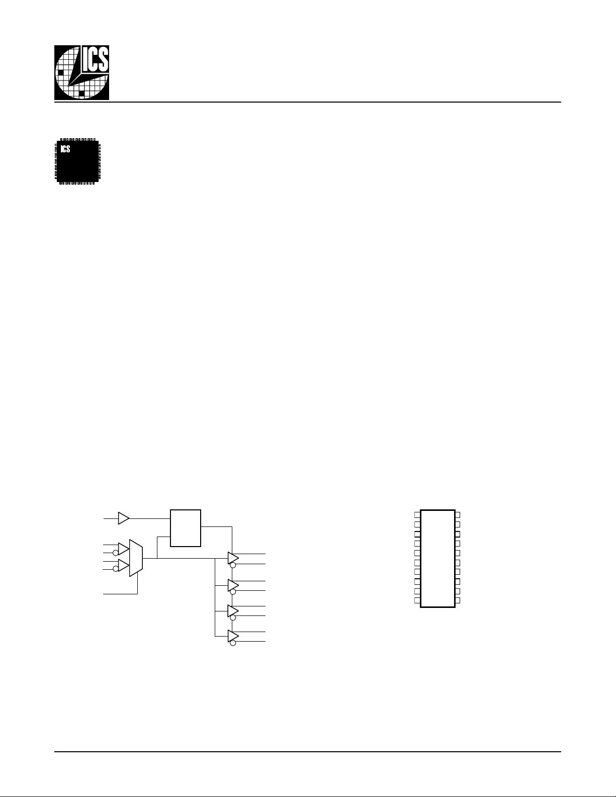
BLOCK DIAGRAM PIN ASSIGNMENT
20
1
CLK_EN
CLK
nCLK
PCLK
nPCLK
CLK_SEL
D
Q
LE
0
1
Q0
nQ0
Q1
nQ1
Q2
nQ2
Q3
nQ3
6.5mm x 4.4mm x 0.92mm body package
GND
CLK_EN
CLK_SEL
CLK
nCLK
PCLK
nPCLK
nc
nc
V
DD
20-Lead TSSOP
2
3
4
5
6
7
8
9
10
ICS8523
G Package
Top View
8523BG www.icst.com/products/hiperclocks.html REV. B JULY 31, 2001
1
19
18
17
16
15
14
13
12
11
Q0
nQ0
V
DDO
Q1
nQ1
Q2
nQ2
V
DDO
Q3
nQ3
Integrated
Circuit
Systems, Inc.
TABLE 1. PIN DESCRIPTIONS
rebmuNemaNepyTnoitpircseD
1DNGrewoP.dnuorgottcennoC.dnuorgylppusrewoP
2NE_KLCtupnIpulluP
3LES_KLCtupnInwodlluP
4KLCtupnInwodlluP.tupnikcolclaitnereffidgnitrevni-noN
5KLCntupnIpulluP.tupnikcolclaitnereffidgnitrevnI
6KLCPtupnInwodlluP.tupnikcolcLCEPVLlaitnereffidgnitrevni-noN
7KLCPntupnIpulluP.tupnikcolcLCEPVLlaitnereffidgnitrevnI
9,8cndesunU.tcennocoN
01V
21,113Q,3QntuptuO.slevelecafretniLTSHVL.riaptuptuolaitnereffiD
81,31V
51,412Q,2QntuptuO.slevelecafretniLTSHVL.riaptuptuolaitnereffiD
71,611Q,1QntuptuO.slevelecafretniLTSHVL.riaptuptuolaitnereffiD
02,910Q,0QntuptuO.slevelecafretniLTSHVL.riaptuptuolaitnereffiD
pulluP
:ETON
DD
ODD
dna
nwodlluP
rewoP.V3.3ottcennoC.nipylppusevitisoP
rewoP.V8.1ottcennoC.snipylppustuptuO
ICS8523
LOW SKEW, 1-TO-4
DIFFERENTIAL-TO-LVHSTL FANOUT BUFFER
kcolcwollofstuptuokcolc,HGIHnehW.elbanekcolcgnizinorhcnyS
decroferastuptuoQn,woldecroferastuptuoQ,WOLnehW.tupni
.slevelecafretniLTTVL/SOMCVL.hgih
KLCPn,KLCPlaitnereffidstceles,HGIHnehW.tupnitceleskcolC
.stupniKLCn,KLCstceles,WOLnehW.stupni
.slevelecafretniLTTVL/SOMCVL
.seulavlacipytrof,scitsiretcarahCniP,2elbaTeeS.srotsisertupnilanretniotsrefer
TABLE 2. PIN CHARACTERISTICS
lobmySretemaraPsnoitidnoCtseTmuminiMlacipyTmumixaMstinU
C
NI
R
PULLUP
R
NWODLLUP
KLCn,KLC4Fp
ecnaticapaCtupnI
rotsiseRpulluPtupnI 15KΩ
rotsiseRnwodlluPtupnI 15KΩ
KLCPn,KLCP4Fp
LES_KLC,NE_KLC4Fp
8523BG www.icst.com/products/hiperclocks.html REV. B JULY 31, 2001
2
Integrated
Circuit
Systems, Inc.
TABLE 3A. CONTROL INPUT FUNCTION TABLE
stupnIstuptuO
NE_KLCLES_KLCecruoSdetceleS3Qurht0Q3Qnurht0Qn
00 KLCn,KLCWOL;delbasiDHGIH;delbasiD
01 KLCPn,KLCPWOL;delbasiDHGIH;delbasiD
10 KLCn,KLCdelbanEdelbanE
11 KLCPn,KLCPdelbanEdelbanE
.1erugiFninwohssa
.B3elbaTni
ICS8523
LOW SKEW, 1-TO-4
DIFFERENTIAL-TO-L VHSTL FANOUT BUFFER
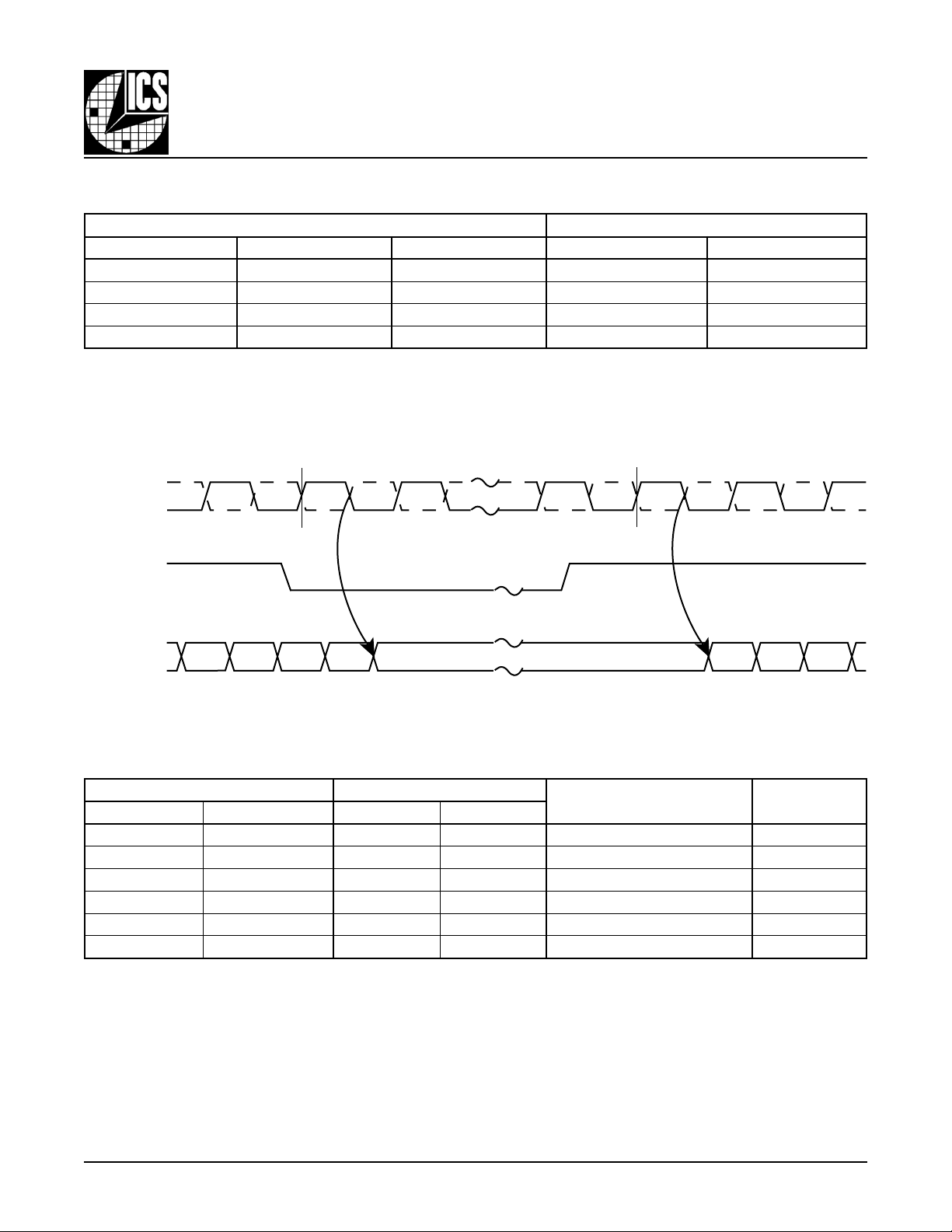
egdekcolctupnignillafdnagnisiragniwollofdelbanerodelbasiderastuptuokcolceht,sehctiwsNE_KLCretfA
debircsedsastupniKLCPn,KLCPdnaKLCn,KLCehtfonoitcnufaerastuptuoehtfoetatseht,edomevitcaehtnI
nCLK, nPCLK
Disabled
CLK, PCLK
CLK_EN
nQ0 - nQ3
Q0 - Q3
TABLE 3B. CLOCK INPUT FUNCTION TABLE
stupnIstuptuO
KLCProKLCKLCPnroKLCn3Qurht0Q3Qnurht0Qn
00WOLHGIHlaitnereffiDotlaitnereffiDgnitrevnInoN
11 HGIHWOLlaitnereffiDotlaitnereffiDgnitrevnInoN
01ETON;desaiBWOLHGIHlaitnereffiDotdednEelgniSgnitrevnInoN
11ETON;desaiBHGIHWOLlaitnereffiDotdednEelgniSgnitrevnInoN
1ETON;desaiB0HGIHWOLlaitnereffiDotdednEelgniSgnitrevnI
1ETON;desaiB1WOLHGIHlaitnereffiDotdednEelgniSgnitrevnI
.sleveldedneelgnistpeccaottupni
Enabled
FIGURE 1 - CLK_EN TIMING DIAGRAM
edoMtuptuOottupnIytiraloP
laitnereffidehtgniriwsessucsidhcihw,9erugiF,8egapnonoitcesnoitamrofnInoitacilppAehtotreferesaelP:1ETON
8523BG www.icst.com/products/hiperclocks.html REV. B JULY 31, 2001
3
Integrated
Circuit
Systems, Inc.
LOW SKEW, 1-TO-4
ICS8523
DIFFERENTIAL-TO-LVHSTL FANOUT BUFFER
ABSOLUTE MAXIMUM RATINGS
Supply Voltage, V
Inputs, V
I
Outputs, V
Package Thermal Impedance, θ
Storage T emperature, T
DDx
O
JA
STG
Stresses beyond those listed under Absolute Maximum Ratings may cause permanent damage to the device. These ratings
are stress specifications only . Functional operation of product at these conditions or any conditions beyond those listed in the
DC Characteristics
or
AC Characteristics
ods may affect product reliability .
4.6V
-0.5V to VDD + 0.5V
-0.5V to V
DDO
+ 0.5V
73.2°C/W
-65°C to 150°C
is not implied. Exposure to absolute maximum rating conditions for extended peri-
TABLE 4A. POWER SUPPLY DC CHARACTERISTICS, V
= 3.3V±5%, V
DD
lobmySretemaraPsnoitidnoCtseTmuminiMlacipyTmumixaMstinU
V
DD
V
ODD
I
DD
egatloVylppuSrewoPtupnI 531.33.3564.3V
egatloVylppuSrewoPtuptuO6.18.10.2V
tnerruCylppuSrewoP 05Am
TABLE 4B. LVCMOS / LVTTL DC CHARACTERISTICS, V
lobmySretemaraPsnoitidnoCtseTmuminiMlacipyTmumixaMstinU
V
HI
V
LI
I
HI
I
LI
TABLE 4C. DIFFERENTIAL DC CHARACTERISTICS, V
lobmySretemaraPsnoitidnoCtseTmuminiMlacipyTmumixaMstinU
I
HI
I
LI
V
PP
V
RMC
2,1ETON
egatloVhgiHtupnILES_KLC,NE_KLC2567.3V
egatloVwoLtupnILES_KLC,NE_KLC3.0-8.0V
tnerruChgiHtupnI
tnerruCwoLtupnI
tnerruChgiHtupnI
tnerruCwoLtupnI
NE_KLCV
LES_KLCV
NE_KLCV
LES_KLCV
= 3.3V±5%, V
DD
KLCnV
KLCV
KLCnV
KLCV
DD
DD
egatloVtupnIkaeP-ot-kaeP 51.03.1V
;egatloVtupnIedoMnommoC
.
VsadenifedsiegatlovedomnommoC:2ETON
= 3.3V±5%, V
DD
DD
DD
DD
DD
V=
DD
NI
V=
DD
NI
= 1.8V±0.2V , TA = 0°C TO 70°C
DDO
= 1.8V±0.2V, TA = 0°C TO 70°C
DDO
V=
NI
V=
NI
DDO
V564.3=5Aµ
V564.3=051Aµ
V,V564.3=
V0=051-Aµ
NI
V,V564.3=
V0=5-Aµ
NI
= 1.8V±0.2V , TA = 0°C TO 70°C
V564.3=5Aµ
V564.3=051Aµ
V,V564.3=
V0=051-Aµ
NI
V,V564.3=
V0=5-Aµ
NI
5.0V
VsiKLCndnaKLCrofegatlovtupnimumixamehtsnoitacilppadedneelgnisroF:1ETON
DD
.V3.0+
58.0-V
DD
8523BG www.icst.com/products/hiperclocks.html REV. B JULY 31, 2001
4
 Loading...