ICS674-01
User Configurable Divider
MDS 674-01 A 1 Revision 033199 Printed 11/15/00
Integrated Circuit Systems • 525 Race Street • San Jose • CA • 95126 •(408)295-9800tel•(408)295-9818fax
PRELIMINARY INFORMATION
• Packaged as 28 pin SSOP (150 mil body)
• Supports ICS673 PLL Building Block
• User determines the divide by setting input pins
• Pull-ups on all select inputs
• Includes one 7-bit Divider for OUTA
• Includes one 9-bit Divider and one selectable
Post Divider for OUTB
• Operating voltages of 3.3 V or 5.0 V
• Industrial temperature range available
• 25mA drive capability at TTL levels
• Advanced, low power CMOS process
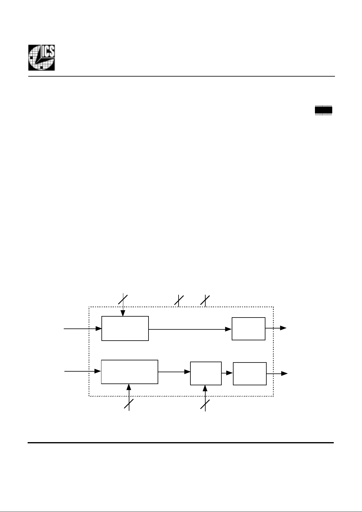
The ICS674-01 consists of 2 separate
configurable dividers. The A Divider is a 7 bit
divider and can divide by 3 to 129. The
B Divider consists of a 9 bit divider followed by a
post divider. The 9 bit divider can divide by 12
to 519. The post divider has eight settings of
1, 2, 4, 5, 6, 7, 8 and 10 giving a maximum total
divide of 5190. The A and B Dividers can be
cascaded to give a maximum divide of 669510.
The ICS674-01 supports the ICS673 PLL
Building Block and enables the user to build a full
custom PLL synthesizer.
Block Diagram
Description
Features
Divider A
(7-Bit)
Output
Buffer
Post
Divider
Divider B
(9-Bit)
7
2
3
VDD GND
INA
INB
OUTA
OUTB
B8:B0
A6:A0
93
S2:S0
Output
Buffer

ICS674-01
User Configurable Divider
MDS 674-01 A 2 Revision 033199 Printed 11/15/00
Integrated Circuit Systems • 525 Race Street • San Jose • CA • 95126 •(408)295-9800tel•(408)295-9818fax
PRELIMINARY INFORMATION
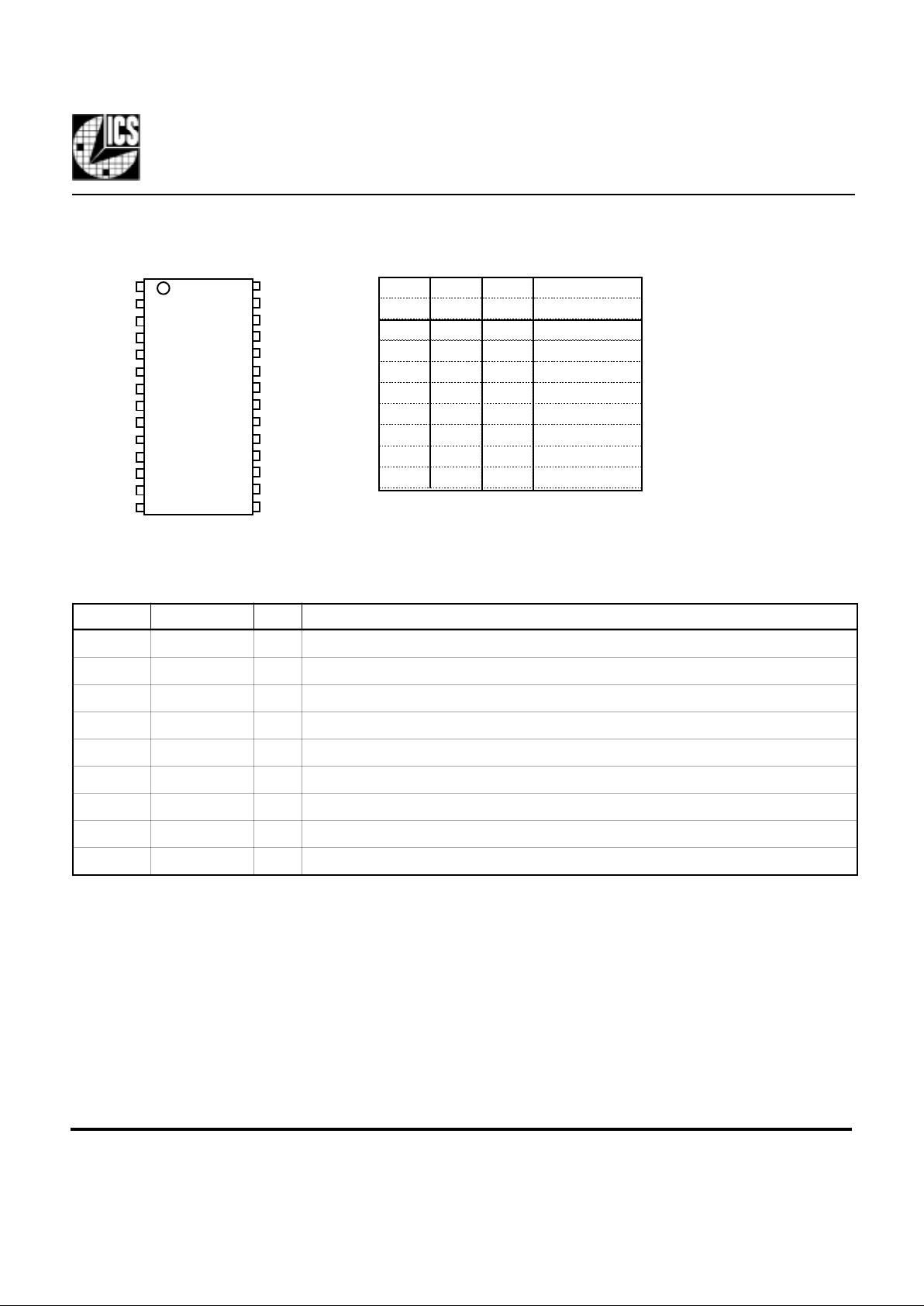
Pin Assignment
Key: I(PU) = Input with internal pull-up resistor; I=Input (no pull-up); O = Output;
P = Power su
pp
ly connection
1
8
9
2
3
4
5
6
7
10
11
12
13
14
16
15
20
17
18
19
25
24
23
22
21
26
27
28
B2
INB
VDD
INA
GND
B4
VDD
OUTA
GND
A2
A4
B8
OUTB
A3
A1
B6
B5
GND
A0
Pin # Name Type Description
1, 2, 24-28 A5, A6, A0-A4 I(PU) Divider A word input pins. Forms a binary number from 3 to 129.
3, 4, 5 S0, S1, S2 I(PU) Select pins for Post Divider. See table above.
6, 23 VDD P Connect to VDD.
7 INA I Divider A input.
8 INB I Divider B input.
9, 19, 20 GND P Connect to ground.
10-18 B0-B8 I(PU) Divider B word input pins. Forms a binary number from 12 to 519.
21 OUTB O Divider B output.
22 OUTA O Divider A output.
A5
A6
B0
B3
B1
S2
S0
S1
B7
S2 S1 S0 Post
pin 5 pin 4 pin 3 Divide
000 10
001 2
010 8
011 4
100 5
101 7
110 1
111 6
Post Divider Table
Pin Description
External Components
The ICS674-01 requires a 0.01µF decoupling capacitor to be connected between VDD and GND. It
must be connected close to the ICS674-01 to minimize lead inductance. Terminating resistors of 33Ω can
be used in series with the OUTA and OUTB
p
ins.
 Loading...