ICS673-01
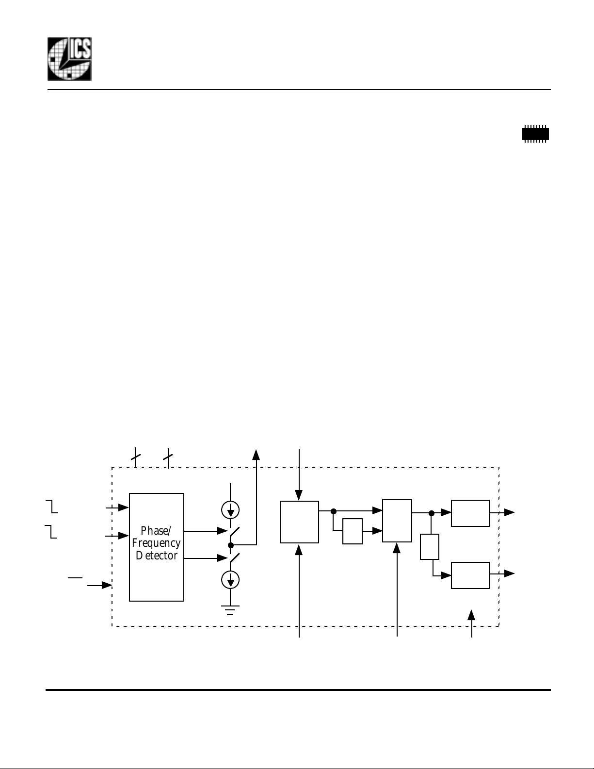
PLL Building Block
Description
The ICS673-01 is a low cost, high performance
Phase Locked Loop (PLL) designed for clock
synthesis and synchronization. Included on the
chip are the phase detector, charge pump, Voltage
Controlled Oscillator (VCO), and two output
buffers. One output buffer is a divide by two of
the other. Through the use of external reference
and VCO dividers (easily implemented with the
ICS674-01), the user can easily customize the
clock to lock to a wide variety of input frequencies.
Included on the ICS673-01 are an Output Enable
function that puts both outputs into a highimpedance state, as well as a Power Down feature
that turns off the entire device.
Features
• Packaged in 16 pin narrow SOIC
• Access to VCO input and feedback paths of PLL
• VCO operating range up to 135 MHz (5V)
• Able to lock MHz range outputs to kHz range
inputs through use of external dividers
• Output Enable tri-states outputs
• Low skew output clocks
• Power Down turns off chip
• VCO predivide of 1 or 4
• 25 mA output drive capability at TTL levels
• Advanced, low power, sub-micron CMOS process
• +3.3 V ±5% or +5 V ±10% operating voltage
• Industrial Temperature range available
• With the ICS674-01, forms a complete PLL
Block Diagram
REFIN
FBIN
PD
(entire chip)
VDD GND
2
3
Phase/
Frequency
Detector
I
UP
DOWN
I
VDD
c
c
CHGP
VCOIN
VCO
CAP
÷ 4
1
MUX
0
SEL
Output
Buffer
÷ 2
Output
Buffer
OE (both outputs)
CLK1
CLK2
MDS 673-01 D 1 Revision 022500 Printed 11/15/00
Integrated Circuit Systems, Inc. • 525 Race Street • San Jose • CA • 95126•(408)295-9800tel • www.icst.com

Pin Assignment
p
ICS673-01
FBIN
VDD
VDD
GND
GND
GND
CHGP
VCOIN
16 pin narrow (150 mil) SOIC
ICS673-01
PLL Building Block
16
1
2
3
4
5
6
7
8
15
14
13
12
11
10
9
REFIN
NC
CLK1
CLK2
PD
SEL
OE
CAP
VCO Predivide Select Table
SEL VCO Predivide
04
11
0 = connect pin directly to ground
1 = connect
in directly to VDD
Pin Descriptions
Number Name Type Description
1 FBIN CI FeedBack INput. Connect feedback clock to this pin. Falling edge triggered.
2 VDD P VDD. Connect to +3.3 V or +5 V, and to VDD on pin 3.
3 VDD P VDD. Connect to VDD on pin 2.
4 GND P Connect to ground.
5 GND P Connect to ground.
6 GND P Connect to ground.
7 CHGP O CHarGe Pump output. Connect to VCOIN under normal operation.
8 VCOIN I Input to internal VCO.
9 CAP I Loop filter return.
10 OE I Output Enable. Active high. Tri-states both outputs when low.
11 SEL I SELect pin for VCO pre-divide per table above.
12 PD I Power Down. Turns off entire chip when this pin is low. Outputs stop low.
13 CLK2 O CLocK output 2. This is a low-skew divide by two version of CLK1.
14 CLK1 O CLocK output 1.
15 NC - No Connect. Nothing is connected internally to this pin.
16 REFIN CI REFerence INput. Connect reference clock to this pin. Falling edge triggered.
Key: CI = clock input, I = Input, O = output, P = power supply connection
MDS 673-01 D 2 Revision 022500 Printed 11/15/00
Integrated Circuit Systems, Inc. • 525 Race Street • San Jose • CA • 95126•(408)295-9800tel • www.icst.com

ICS673-01
V
V
PLL Building Block
Electrical Specifications
Parameter Conditions Minimum Typical Maximum Units
ABSOLUTE MAXIMUM RATINGS (note 1)
Supply voltage, VDD Referenced to GND 7 V
Inputs and Clock Outputs Referenced to GND -0.5 VDD+0.5 V
Ambient Operating Temperature ICS673M-01 0 70 °C
ICS673M-01I -40 85 °C
Soldering Temperature Max of 10 seconds 260 °C
Storage temperature -65 150 °C
DC CHARACTERISTICS (VDD = 5.0 V unless noted)
Operating Voltage, VDD 3.13 5.50 V
Input High Voltage
Input Low Voltage
Input High Voltage
Input Low Voltage
Output High Voltage, VOH IOH=-25mA 2.4 V
Output Low Voltage, VOL IOL=25mA 0.4 V
Output High Voltage, VOH, CMOS level IOH=-8mA VDD-0.4 V
Operating Supply Current, IDD No Load,CLK1=40MHz 15 mA
Power Down Supply Current, IDDPD No Load 6 µA
Short Circuit Current Each output ±100 mA
Input Capacitance OE, PD, SEL 5 pF
AC CHARACTERISTICS (VDD = 5.0
Output Clock Frequency (4.5 to 5.5 V) CLK1 with SEL=1 2
Output Clock Frequency (3.13 to 3.46 V) CLK1 with SEL=1 2
CLK1 and CLK2 skew Rising edges at VDD/2 500 ps
Output Clock Rise Time 0.8 to 2.0V 1.5 ns
Output Clock Fall Time 2.0 to 0.8V 1.5 ns
Output Clock Duty Cycle At VDD/2 45 50 55 %
VCO Gain, Kv 95 MHz/V
Charge Pump Current, Ic 2.4 µA
Notes: 1. Stresses beyond those listed under Absolute Maximum Ratings could cause permanent damage to the device. Prolonged
exposure to levels above the operating limits but below the Absolute Maximums may affect device reliability.
All except VCOIN
All except VCOIN
VCOIN
VCOIN
unless noted)
2 V
0.8 V
VDD V
0 V
135 MHz
100 MHz
MDS 673-01 D 3 Revision 022500 Printed 11/15/00
Integrated Circuit Systems, Inc. • 525 Race Street • San Jose • CA • 95126•(408)295-9800tel • www.icst.com
 Loading...