ICS671-01
Zero Delay, Low Skew Buffer and Multipler
Description
The ICS671-01 is a low phase noise, high speed
PLL based, 8 output, low skew zero delay buffer
and multiplier. Based on ICS’s proprietary low
jitter Phase Locked Loop (PLL) techniques, the
device provides eight low skew outputs at speeds
up to 160 MHz at 3.3 V. The ICS671-01 includes
a bank of six outputs running at either x2 or x4
mode, one output running at either x2, x4, or x5
mode, and one more output running at either x1,
x2, or x4 mode. For normal operation, output
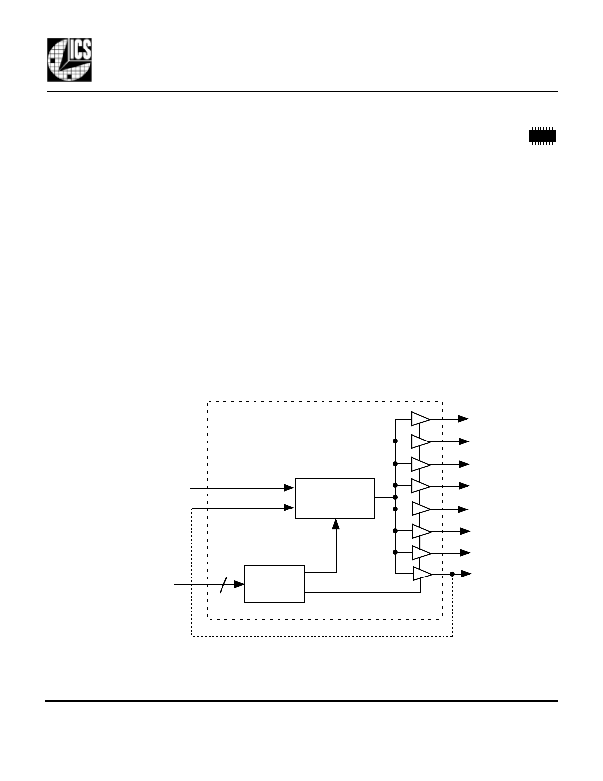
clock CLK8 is tied to the FBIN pin.
ICS manufactures the largest variety of clock
generators and buffers, and is the largest clock
supplier in the world.
Block Diagram
Features
• Packaged in 16 pin narrow SOIC
• Clock outputs from 5 to 160 MHz
• Zero input-output delay
• Integrated x2 or x4 selections, and x5 for CLK7
• Eight low-skew (<250 ps) outputs
• Full CMOS outputs with 25 mA output drive
capability at TTL levels
• Tri-state mode for board-level testing
• Advanced, low power, sub-micron CMOS process
• 3.3 V to 5 V operating voltage
CLKIN
FBIN
S1, S0
CLK1
CLK2
CLK3
x2, x4, or x5
PLL
2
Control
Logic
CLK4
CLK5
CLK6
CLK7
CLK8
MDS 671-01 B 1 Revision 051700 Printed 11/15/00
Integrated Circuit Systems, Inc.• 525 Race Street • San Jose •CA•95126• (408) 295-9800 tel • www.icst.com

ICS671-01
Zero Delay, Low Skew Buffer and Multipler
Pin Assignment
ICS671-01
16
1
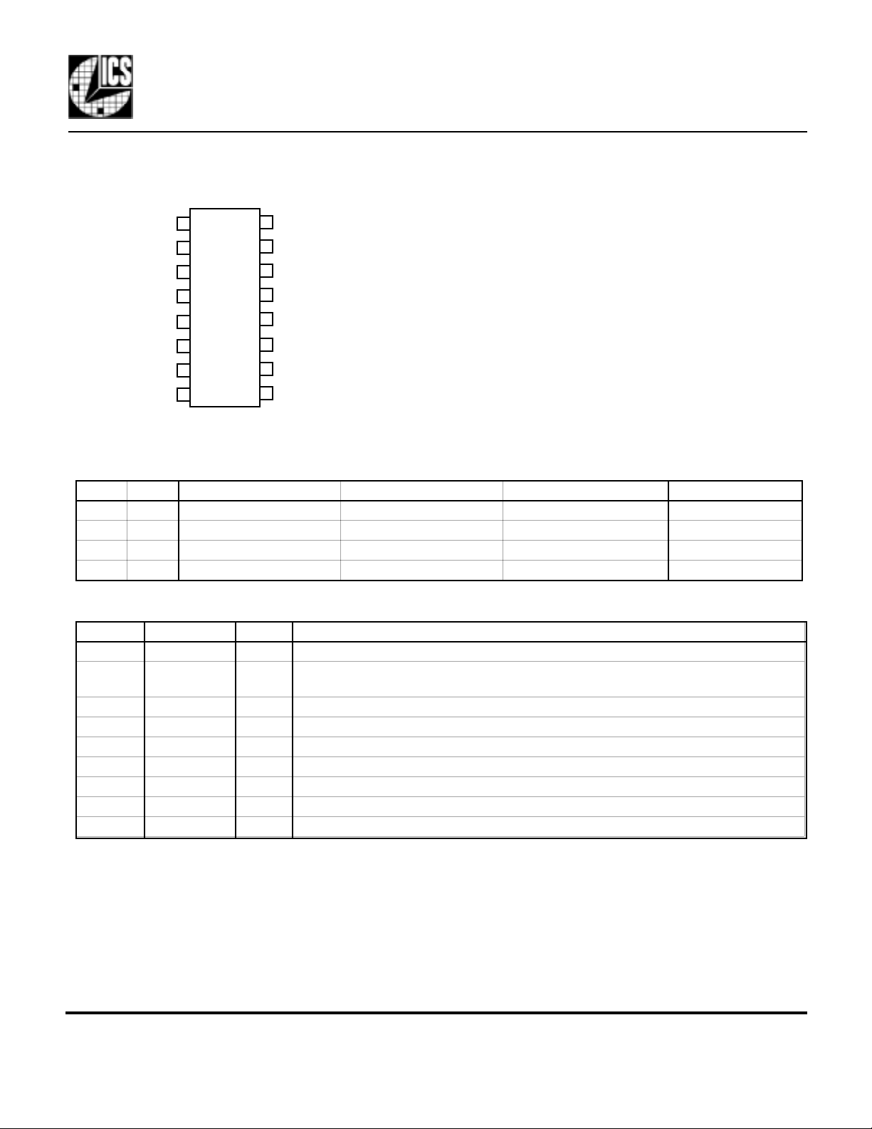
CLK1
2
3
VDD
GND
CLK3
CLK4
S0
4
5
6
7
8
16 pin narrow (150 mil) SOIC
Output Clock Mode Select Table
S1 S0 CLK1:6 CLK7 CLK8 Input range
0 0 Tri-state (high impedance) Tri-state (high impedance) Tri-state (high impedance) 0 1 x2 x5 x1 5 to 30 MHz
1 0 x 2 x2 x2 15 to 80 MHz
1 1 x4 x 4 x4 7.5 to 40 MHz
15
14
13
12
11
10
9
FBINCLKIN
CLK8
CLK7CLK2
VDD
GND
CLK6
CLK5
S1
Pin Descriptions
Number Name Type Description
1 CLKIN I Clock Input.
2, 3, 6, 7,
10, 11
4, 13 VDD P Power supply. Connect both pins to same voltage (either 3.3 V or 5 V).
5, 12 GND P Connect to ground.
8 S0 I Select input 0. See table above.
9 S1 I Select input 1. See table above.
14 CLK7 I Clock Output 7. See table above.
15 CLK8 I Clock Output 8. See table above. Normally use this clock as feedback.
16 FBIN I Feedback Input. Connect to CLK8 under normal operations.
CLK1:6 O Clock Outputs 1:6. See above table.
Key: I = Input; O = output; P = power supply connection.
External Components
The ICS671-01 requires a minimum number of external components for proper operation. Decoupling
capacitors of 0.01µF should be connected between VDD and GND on pins 4 and 5, and VDD and GND
on pins 13 and 12, as close to the device as possible. A series termination resistor of 33 Ω may be used close
to each clock output pin to reduce reflections.
MDS 671-01 B 2 Revision 051700 Printed 11/15/00
Integrated Circuit Systems, Inc.• 525 Race Street • San Jose •CA•95126• (408) 295-9800 tel • www.icst.com
 Loading...