Low Phase Noise Zero Delay Buffer and Multiplier
p
Description Features
The ICS670-01 is a high speed, low phase noise
Zero Delay Buffer (ZDB) which integrates ICS’
proprietary analog/digital Phase Locked Loop
(PLL) techniques. Part of ICS’ ClockBlocks
family, the zero delay feature means that the rising
edge of the input clock aligns with the rising edges
of the outputs, giving the appearance of no delay
through the device. There are two identical outputs
on the chip. The FBCLK should be used to
connect to the FBIN. Each output has its own
output enable pin.
™
• Packaged in 16 pin SOIC
• Clock inputs from 5 to 160 MHz (see page 2)
• Patented PLL with the lowest phase noise
• Output clocks up to 160 MHz at 3.3 V
• 15 selectable on-chip multipliers
• Power down mode available
• Low phase noise: -124 dBc/Hz at 10 kHz
• Output Enable function tri-states outputs
ICS670-01
The chip is ideal for synchronizing outputs in a
large variety of systems, from personal computers
to data communications to video. By allowing offchip feedback paths, the ICS670-01 can eliminate
the delay through other devices. The 15 different
on-chip multipliers work in a variety of
applications. For other multipliers, including
fractional multipliers, see the ICS527.
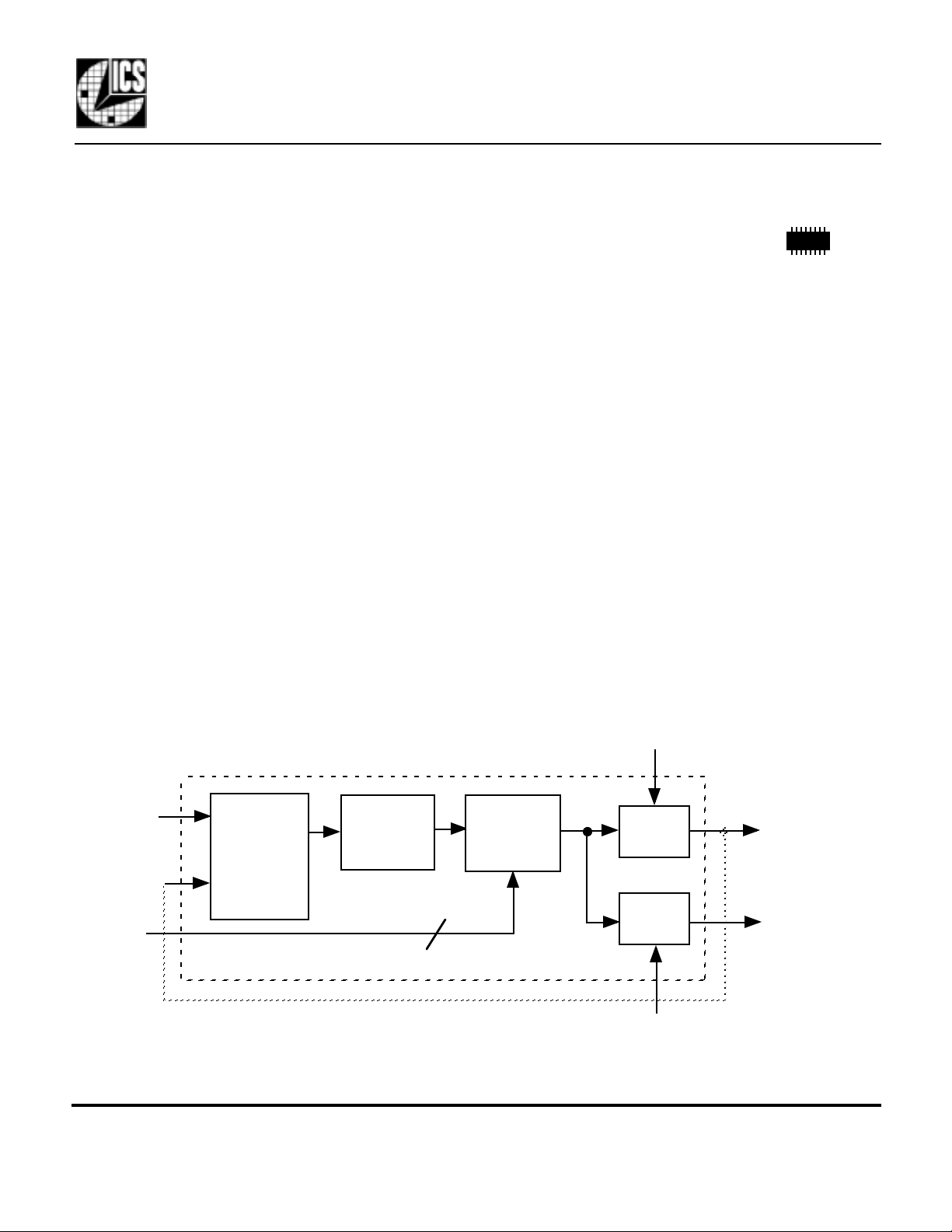
Block Diagram
ICLK
FBIN
S3:S0
Phase
Detector,
Charge
Pump, and
Loop Filter
Voltage
Controlled
Oscillator
4
• Low jitter 15 ps one sigma
• Full swing CMOS outputs with 25 mA drive
capability at TTL levels
• Advanced, low power, sub-micron CMOS process
• Industrial temperature version available
• 3.3 V or 5 V operation
OE1
ROM-
Based
Multi
liers
Output
Buffer
Output
Buffer
FBCLK
CLK2
External feedback from FBCLK is recommended.
MDS 670-01 B 1 Revision 100900 Printed 11/15/00
Integrated Circuit Systems • 525 Race Street • San Jose •CA•95126•(408) 295-9800tel•http://www.icst.com
OE2

ICS670-01
Low Phase Noise Zero Delay Buffer and Multiplier
Pin Assignment
VDD
VDD
VDD
CLK2
OE2
FBCLK
OE1
FBIN
1
2
3
4
5
6
7
8
ICS670-01
Pin Descriptions
16
15
14
13
12
11
10
Multiplier Select Table
S3 S2 S1 S0 CLK2 (and FBCLK) Input Range (MHz)
GND
GND
GND
S0
S1
S2
S3
ICLK
9
0000 Low (Power down entire chip) 0001 Input x1.333 18 - 12 0
0010 Input x6 5 - 26.67
0011 Input x1.5 16.67 - 107
0100 Input x3.333 7.5 - 48
0101 Input x2.50 10 - 6 4
0110 Input x4 6 - 4 0
0111 Input x1 25 - 1 6 0
1000 Input x2.333 11 - 6 9
1001 Input x2.666 10 - 6 0
1010 Input x12 5 - 13.33
1011 Input x3 8 - 53.33
1100 Input x10 5 - 16
1101 Input x5 6 - 32
1110 Input x8 5 - 20
1111 Input x2 12 - 8 0
0=connect directly to ground
1=connect directl to VDD
Number Name Type Description
1 VDD P Connect to +3.3V or +5V. Must match other VDDs.
2 VDD P Connect to +3.3V or +5V. Must match other VDDs.
3 VDD P Connect to +3.3V or +5V. Must match other VDDs.
4 CLK2 O Clock output from VCO. Output frequency equals the input frequency times multiplier.
5 OE2 I Output clock enable 2. Tri-states the clock 2 output when low.
6 FBCLK O Clock ouput from VCO. Output frequency equals the input frequency times multiplier.
7
8 FBIN CI Feedback clock input.
9 ICLK CI Clock input. Connect to a 5 - 160 MHz clock.
10 S3 I Multiplier select pin 3. Determines outputs per table above. Internal pull-up.
11 S2 I Multiplier select pin 2. Determines outputs per table above. Internal pull-up.
12 S1 I Multiplier select pin 1. Determines outputs per table above. Internal pull-up.
13 S0 I Multiplier select pin 0. Determines outputs per table above. Internal pull-up.
14 GND P Connect to ground.
15 GND P Connect to ground.
16 GND P Connect to ground.
OE1 I Output clock enable 1. Tri-states the feedback clock output when low.
Key: I = Input with internal pull-up resistor; O = output; P = power supply connection; CI = clock input.
MDS 670-01 B 2 Revision 100900 Printed 11/15/00
Integrated Circuit Systems • 525 Race Street • San Jose •CA•95126•(408) 295-9800tel•http://www.icst.com
 Loading...