

PRELIMINARY INFORMATION
System Peripheral Clock Source
ICS650-21
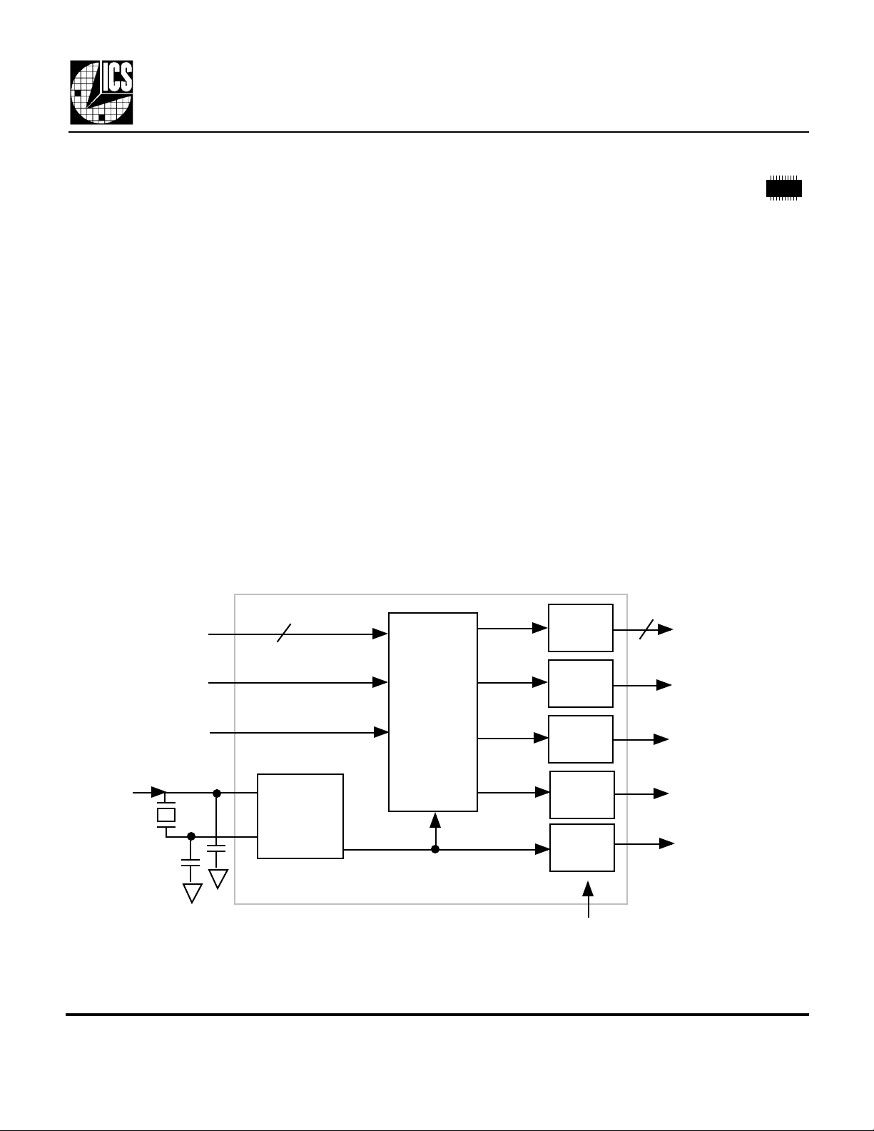
Description
The ICS650-21 is a low cost, low jitter, high
performance clock synthesizer for system
peripheral applications. Using analog/digital
Phase-Locked Loop (PLL) techniques, the device
accepts a parallel resonant 25 MHz crystal input to
produce up to eight output clocks. The device
provides clocks for PCI, SCSI, Fast Ethernet,
Ethernet, USB, and AC97. The user can select one
of three USB frequencies, and also one of two
AC97 audio frequencies. The OE pin puts all
outputs into a high impedance state for board level
testing. All frequencies are generated with less than
one ppm error, meeting the demands of SCSI and
Ethernet clocking.
The ICS650 can be mask customized to produce
any frequencies from 1 to 150 MHz.
Block Diagram
Features
• Packaged in 20 pin tiny SSOP (QSOP)
• Lower jitter version of ICS650-01
• Operating VDD of 3.3V or 5V
• Zero ppm synthesis error in all clocks
• Inexpensive 25 MHz crystal or clock input
• Provides Ethernet and Fast Ethernet clocks
• Provides SCSI clocks
• Provides PCI clocks
• Selectable AC97 audio clock
• Selectable USB clock
• OE pin tri-states the outputs for testing
• Selectable frequencies on three clocks
• Duty cycle of 45/55 for Processor clock and Audio
clock
• Advanced, low power CMOS process
PSEL1:0
ASEL
USEL
25 MHz
crystal
or clock
MDS 650-21 A 1 Revision 010301
Integrated Circuit Systems, Inc. • 525 Race Street • San Jose •CA•95126• (408) 295-9800tel • www.icst.com
X1/ICLK
X2
2
Clock
Synthesis
Circuitry
Crystal
Oscillator
Output
Buffer
Output
Buffer
Output
Buffers
Output
Buffers
Output
Buffer
Output Enable (all outputs)
3
Processor Clocks
(Fast Ethernet,
SCSI, PCI )
Audio Clock
USB Clock
20 MHz
25 MHz
PRELIMINARY INFORMATION
System Peripheral Clock Source
ICS650-21
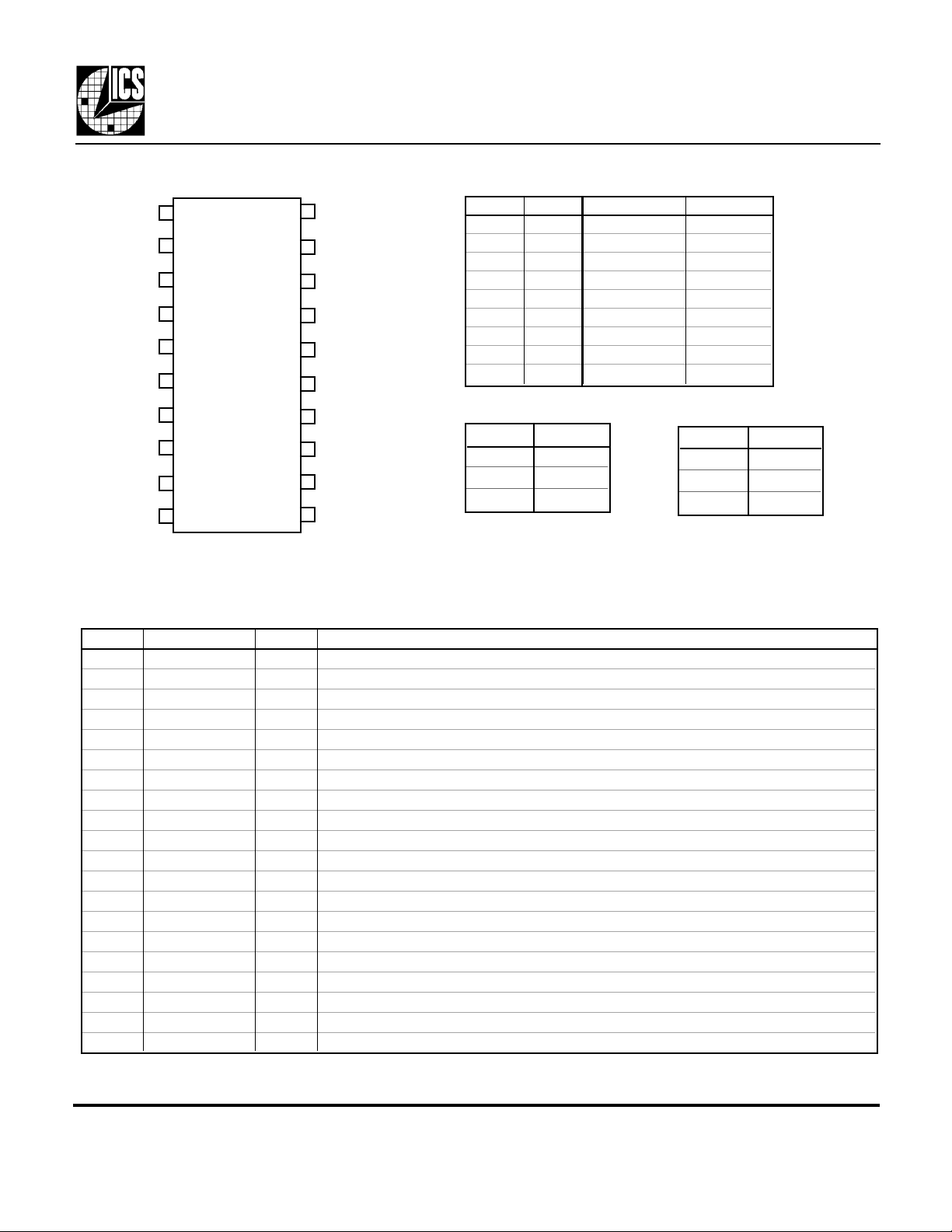
Pin Assignment
USEL
X2
X1/ICLK
VDD
VDD
GND
UCLK
20M
ACLK
25M
1
2
3
4
5
6
7
8
9
10
20
19
18
17
16
15
14
13
12
11
PSEL1
PSEL0
PCLK2
PCLK3
VDD
ASEL
GND
OFF/14.318M
PCLK1
OE
Processor Clock (MHz)
PSEL1 PSEL0 PCLK1 PCLK2,3
0 0 25.00 50.00
0 M 37.5 75.00
0 1 66.66 133.33
M 0 40.00 80.00
M M 33.3334 66.6667
M 1 20.00 40.00
1 0 20.00 33.3334
1 M 20.00 66.6667
1 1 50 100
Audio Clock (MHz)
ASEL ACLK
0 49.152
M 24.576
1 14.318
USB Clock (MHz)
USEL UCLK
0 12
M 24
1 48
0 = connect directly to ground, 1 = connect directly
20 pin (150 mil) SSOP
to VDD, M=leave unconnected (floating)
Pin Descriptions
Pin # Name Type Description
1 USEL I UCLK Select pin. Determines frequency of USB clock per table above.
2 X2 XO Crystal connection. Connect to parallel mode 25 MHz crystal. Leave open for clock.
3 X1/ICLK XI Crystal connection. Connect to parallel mode 25 MHz crystal, or clock.
4 VDD P Connect to VDD. Must be same value as other VDD. Decouple with pin 6.
5 VDD P Connect to VDD. Must be same value as other VDD.
6 GND P Connect to ground.
7
8 20M O Fixed 20 MHz output for Ethernet.
9 ACLK O AC97 Audio clock output per table above.
10 25M O Fixed 25 MHz reference output for Fast Ethernet.
11 OE I Output Enable. Tri-states all outputs when low.
12 PCLK1 O PCLK output number 1 per table above.
13 OFF/14.318M O 14.31818 MHz clock output only when ASEL=VDD.
14 GND P Connect to ground.
15 ASEL I ACLK Select pin. Determines frequency of Audio clock per table above.
16 VDD P Connect to VDD. Must be same value as other VDD. Decouple with pin 14.
17 PCLK3 O PCLK output number 3 per table above.
18 PCLK2 O PCLK output number 2 per table above.
19 PSEL0 I Processor Select pin #0. Determines frequencies on PCLKs 1-3 per table above.
20 PSEL1 I Processor Select pin #1. Determines frequencies on PCLKs 1-3 per table above.
UCLK O USB clock output per table above.
Key: I = Input; XO/XI = crystal connections; O = output; P = power supply connection
MDS 650-21 A 2 Revision 010301
Integrated Circuit Systems, Inc. • 525 Race Street • San Jose •CA•95126• (408) 295-9800tel • www.icst.com

PRELIMINARY INFORMATION
ABSOLUTE MAXIMUM RATINGS (note 1)
DC CHARACTERISTICS (VDD = 3.3V or 5V unless noted)
AC CHARACTERISTICS (VDD = 3.3V or 5V unless noted)
exposure to levels above the operating limits but below the Absolute Maximums may affect device reliability.
2. With all clocks at highest frequencies.
ICS650-21
System Peripheral Clock Source
Electrical Specifications
Parameter Conditions Minimum Typical Maximum Units
Supply voltage, VDD Referenced to GND 7 V
Inputs and Clock Outputs Referenced to GND -0.5 VDD+0.5 V
Ambient Operating Temperature 0 70 C
Soldering Temperature Max of 10 seconds 260 C
Storage temperature -65 150 C
Operating Voltage, VDD 3.0 5.5 V
Input High Voltage, VIH Select inputs, OE 2 V
Input Low Voltage, VIL Select inputs, OE 0.8 V
Output High Voltage, VOH VDD=3.3V, IOH=-8mA 2.4 V
Output Low Voltage, VOL VDD=3.3V, IOL=8mA 0.4 V
Output High Voltage, VOH, VDD = 3.3 or 5V IOH=-8mA VDD-0.4 V
Operating Supply Current, IDD, at 5V No Load, note 2 50 mA
Operating Supply Current, IDD, at 3.3V No Load, note 2 30 mA
Short Circuit Current, VDD = 3.3 Each output ±50 mA
Input Capacitance Except X1 5 pF
Input Crystal or Clock Frequency 25.000 MHz
Output Clocks Accuracy (synthesis error) All clocks 1 ppm
Output Clock Rise Time 0.8 to 2.0V 1.5 ns
Output Clock Fall Time 2.0 to 0.8V 1.5 ns
Output Clock Duty Cycle, UCLCK At VDD/2 40 50 60 %
Output Clock Duty Cycle, PCLCK, ACLCK At VDD/2 45 50 55 %
One Sigma Jitter, except ACLK 75 ps
One Sigma Jitter, ACLK 120 ps
Absolute Clock Period Jitter PCLK, UCLK, 20M
Notes: 1. Stresses beyond those listed under Absolute Maximum Ratings could cause permanent damage to the device. Prolonged
- 500 500 ps
External Components
The ICS650 requires a minimum number of external components for proper operation. Decoupling
capacitors of 0.1µF should be connected between VDD and GND (on pins 4 and 6, and pins 16 and 14),
as close to the chip as possible. A series termination resistor of 33Ω may be used for each clock output. The
25.000 MHz crystal must be connected as close to the chip as possible. The crystal should be a fundamental
mode, parallel resonant, 30ppm or better (to meet the Ethernet specs). Crystal capacitors should be
connected from pins X1 to ground and X2 to ground. The value of these capacitors is given by the
following equation, where CL is the crystal load capacitance: Crystal caps (pF) = (CL-12) x 2. So for a
crystal with 16pF load capacitance, two 8pF caps should be used. If a clock input is used, drive it into X1
and leave X2 unconnected.
MDS 650-21 A 3 Revision 010301
Integrated Circuit Systems, Inc. • 525 Race Street • San Jose •CA•95126• (408) 295-9800tel • www.icst.com

PRELIMINARY INFORMATION
AREA
Inches
Millimeters
System Peripheral Clock Source
Package Outline and Package Dimensions
(For current dimensional specifications, see JEDEC Publication No. 95.)
20 pin SSOP
Symbol Min Max Min Max
A 0.053 0.069 1.35 1.75
A1 0.004 0.010 0.10 0.25
E1 E
INDEX
1 2
D
b 0.008 0.012 0.20 0.30
c 0.007 0.010 0.18 0.25
D 0.337 0.344 8.55 8.75
e
E 0.228 0.244 5.80 6.20
E1 0.150 0.157 3.80 4.00
L 0.016 0.050 0.40 1.27
ICS650-21
A1 c
A
e
b
L
Ordering Information
Part/Order Number Marking Package Shipping Temperature
ICS650R-21 ICS650R-21 20 pin SSOP Tubes 0 to 70° C
ICS650R-21T ICS650R-21 20 pin SSOP Tape and Reel 0 to 70° C
ICS650R-21I ICS650R-21I 20 pin SSOP Tubes -40 to 85° C
ICS650R-21IT ICS650R-21I 20 pin SSOP Tape and Reel -40 to 85° C
While the information presented herein has been checked for both accuracy and reliability, Integrated Circuit Systems, Incorporated (ICS) assumes no responsibility for either its
use or for the infringement of any patents or other rights of third parties, which would result from its use. No other circuits, patents, or licenses are implied. This product is
intended for use in normal commercial applications. Any other applications such as those requiring extended temperature range, high reliability, or other extraordinary
environmental requirements are not recommended without additional processing by ICS. ICS reserves the right to change any circuitry or specifications without notice. ICS does
not authorize or warrant any ICS product for use in life support devices or critical medical instruments.
MDS 650-21 A 4 Revision 010301
Integrated Circuit Systems, Inc. • 525 Race Street • San Jose •CA•95126• (408) 295-9800tel • www.icst.com
 Loading...