PRELIMINARY INFORMATION
Networking Clock Source
ICS650-07C
Description
The ICS650-07C is a low cost, low jitter, high
performance clock synthesizer for networking
applications. Using analog Phase-Locked Loop
(PLL) techniques, the device accepts a 12.5 MHz
or 25.00 MHz clock or fundamental mode crystal
input to produce multiple output clocks for
networking chips, PCI devices, SDRAM, and
ASICs. The ICS650-07C outputs all have 0 ppm
synthesis error.
See the MK74CB214, ICS551, and ICS552-01 for
non-PLL buffer devices which produce multiple
low-skew copies of these output clocks.
See the ICS570, ICS9112-16/17/18 for zero delay
buffers that can synchronize outputs and other
needed clocks.
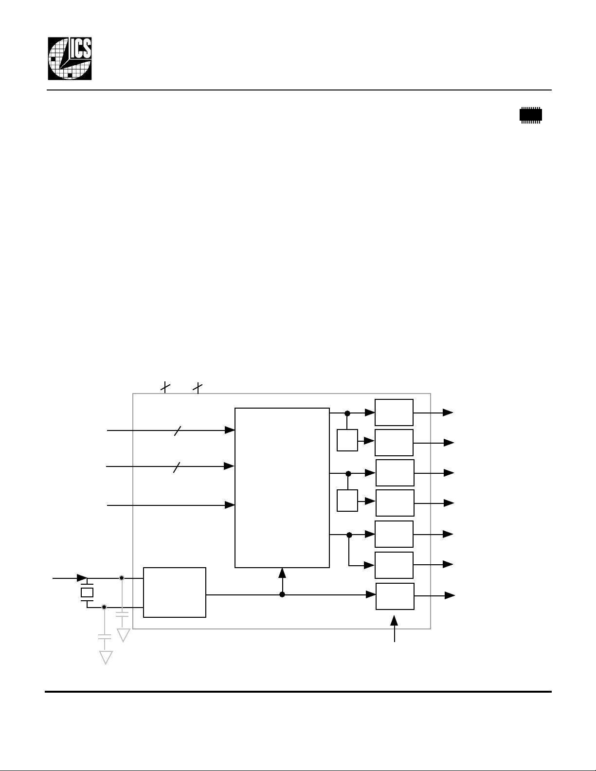
Block Diagram
VDD
GND
2
2
Features
• Packaged in 20 pin narrow (150 mil) SSOP (QSOP)
• 12.5 MHz or 25.00 MHz fundamental crystal or
clock input
• Six output clocks with selectable frequencies
• SDRAM frequencies of 67, 83, 100, and 133 MHz
• Buffered crystal reference output
• Zero ppm synthesis error in all clocks
• Ideal for PMC-Sierra’s ATM switch chips
• Full CMOS output swing with 25 mA output drive
capability at TTL levels
• Advanced, low power, sub-micron CMOS process
• 3.0V to 5.5V operating voltage
ACS1,0
BCS1,0
CCS
12.5 MHz or
25.00 MHz
crystal or clock
X1
X2
2
2
Clock
Buffer/
Crystal
Oscillator
Clock Synthesis
and Control
Circuitry
÷ 2
÷ 2
Output
Buffer
Output
Buffer
Output
Buffer
Output
Buffer
Output
Buffer
Output
Buffer
Output
Buffer
CLKA1
CLKA2
CLKB1
CLKB2
CLKC1
CLKC2
REFOUT
OE (all outputs)
Optional crystal capacitors are shown and may be required for tuning of initial accuracy (determined once per board).
MDS 650-07C A 1 Revision 101399 Printed 11/28/00
Integrated Circuit Systems, Inc. • 525 Race Street • San Jose • CA • 95126•(408)295-9800tel • www.icst.com

PRELIMINARY INFORMATION
Networking Clock Source
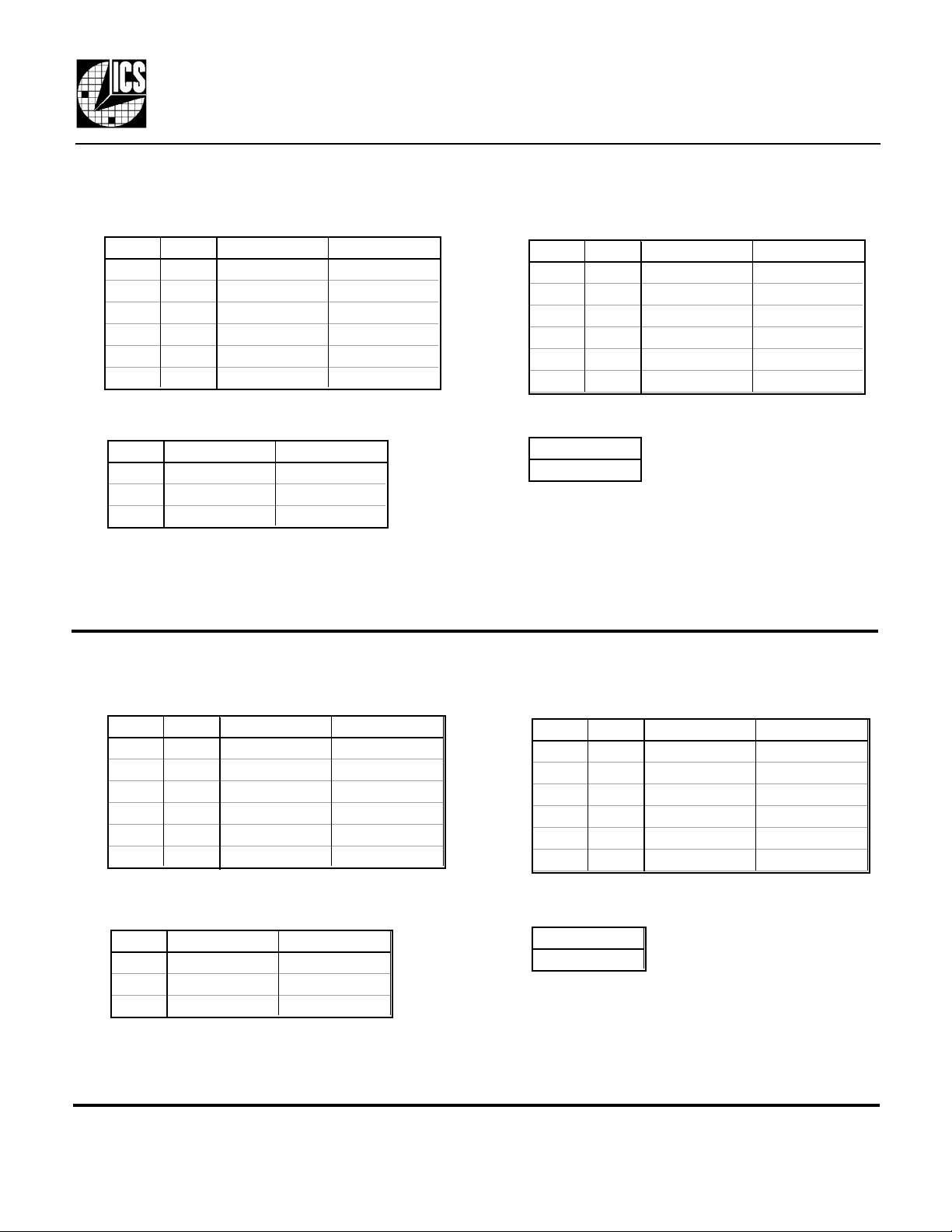
For a 25 MHz fundamental crystal or clock input, the following four tables apply :
ICS650-07C
A Clocks Select Table (outputs in MHz)
ACS1 ACS0 CLKA1 CLKA2
0 0 100 off (low)
0 M Test Test
0 1 75 off (low)
1 0 33.3333 16.6667
1 M Test Test
1 1 66.6667 33.3333
B Clocks Select Table (outputs in MHz)
BCS1 BCS0 CLKB1 CLKB2
0 0 Test Test
0 M 66.6667 33.3333
0 1 100 50
1 0 83.3333 41.6667
1 M Test Test
1 1 133.3333 66.6667
C Clocks Select Table (outputs in MHz)
CCS CLKC1 CLKC2
0 125 125
M Test Test
1 75 75
0 = connect directly to GND
M = leave unconnected (automatically self biases to VDD/2)
1 = connect directly to VDD
REFOUT
25 MHz
For a 12.5 MHz crystal or clock input, the following four tables apply :
A Clocks Select Table (outputs in MHz)
ACS1 ACS0 CLKA1 CLKA2
0 0 50 off (low)
0 M Test Test
0 1 37.5 off (low)
1 0 16.6667 8.3333
1 M Test Test
1 1 33.3333 16.6667
B Clocks Select Table (outputs in MHz)
BCS1 BCS0 CLKB1 CLKB2
0 0 Test Test
0 M 33.3333 16.6667
0 1 50 25
1 0 41.6667 20.8333
1 M Test Test
1 1 66.6667 33.3333
C Clocks Select Table (outputs in MHz)
CCS CLKC1 CLKC2
0 62.5 62.5
M Test Test
1 37.5 37.5
0 = connect directly to GND
M = leave unconnected (automatically self biases to VDD/2)
1 = connect directly to VDD
MDS 650-07C A 2 Revision 101399 Printed 11/28/00
REFOUT
12.5 MHz
Integrated Circuit Systems, Inc. • 525 Race Street • San Jose • CA • 95126•(408)295-9800tel • www.icst.com
 Loading...