PRELIMINARY
PRELIMINARY
INFORMATION
INFORMATION
Description Features
ICS650-05
HDTV Clock Synthesizer
The ICS650-05 is a low cost, low jitter, high
performance clock synthesizer designed to
produce 74.175824 MHz and 74.250000 MHz as
necessary for HDTV applications. Using our
patented analog Phase-Locked Loop (PLL)
techniques, the device uses a 27.0 MHz clock or
fundamental crystal input to produce buffered,
fixed clocks and a selectable frame rate clock for
HDTV systems.
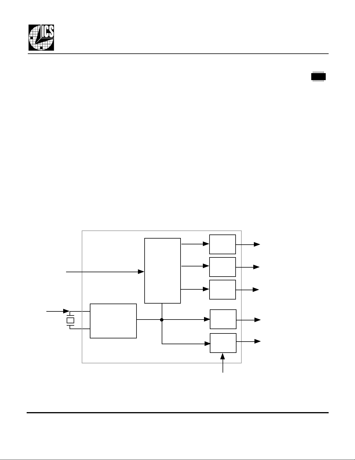
Block Diagram
Clock
Synthesis
FRS
and
Control
Circuit
• Packaged in 20 pin tiny SSOP (QSOP)
• Input Frequency of 27.0 MHz
• Zero ppm synthesis error in output clocks
• Provides fixed 13.5 MHz, dual 27.0 MHz, and
54.0 MHz output clocks with a selectable Frame
Rate Clock of 74.175824 MHz or
74.250000 MHz
• Ideal for HDTV applications
• 3.3 V or 5.0 V operating voltage
Output
Buffer
Output
Buffer
Output
Buffers
FRCLK
54.0 MHz
13.5 MHz
Input
27.0 MHz
MDS 650-05 A 1 Revision 081199 Printed 12/4/00
Integrated Circuit Systems • 525 Race Street • San Jose •CA•95126• (408) 295-9800tel • (408) 295-9818fax
Buffer/Crystal
Oscillator
Output
Buffers
Output
Buffer
OE (all outputs)
27.0 MHz
27.0 MHz

Pin Assignment
PRELIMINARY
PRELIMINARY
INFORMATION
INFORMATION
HDTV Clock Synthesizer
ICS650-05
VDD
X2
X1/ICLK
VDD
VDD
GND
NC
27M
13.5M
GND
1
2
3
4
5
6
7
8
9
20
19
18
17
16
15
14
13
12
1110
VDD
OE
FRS
FRCLK
VDD
GND
GND
54M
27M
GND
FRCLK Output Select Table (in MHz)
FRS Pin 18 FRCLK Pin 17
0 74.175824
1 74.250000
20 pin SSOP (QSOP)
Pin Descriptions
Pin # Name Type Description
1 VDD P Connect to +3.3 V or +5.0 V. Must be same as other VDDs.
2 X2 XO Crystal connection to a 27.0 MHz crystal or leave unconnected for clock input
3 X1/ICLK XI Crystal connection. Connect to a 27.0 MHz fundamental mode crystal or clock input.
4 VDD P Connect to +3.3 V or +5.0 V. Must be same as other VDDs.
5 VDD P Connect to +3.3 V or +5.0 V. Must be same as other VDDs.
6 GND P Connect to ground.
7 NC - No Connect. Do not connect anything to this pin.
8 27M O 27 MHz buffered oscillator clock output.
9 13.5M O 13.5 MHz clock output.
10 GND P Connect to ground.
11 GND P Connect to ground.
12 27M O 27 MHz buffered clock output.
13 54M O 54 MHz buffered clock output.
14 GND P Connect to ground.
15 GND P Connect to ground.
16 VDD P Connect to +3.3 V or +5.0 V. Must be same as other VDDs.
17 FRCLK O Frame Rate Clock as shown on table.
18 FRS I Frame Rate Frequency Select input pin. Determines FRCLK output as shown on table.
19 OE I Output Enable. Tri-states all clocks when low.
20 VDD P Connect to +3.3 V or +5.0 V. Must be same as other VDDs.
Key: I = Input with internal pull-up; O = output; P = power supply connection; XI, XO = crystal
connections
MDS 650-05 A 2 Revision 081199 Printed 12/4/00
Integrated Circuit Systems • 525 Race Street • San Jose •CA•95126• (408) 295-9800tel • (408) 295-9818fax
 Loading...