ICS650-01
System Peripheral Clock Source
Description
The ICS650-01 is a low cost, low jitter, high
performance clock synthesizer for system
peripheral applications. Using analog/digital
Phase-Locked Loop (PLL) techniques, the device
accepts a parallel resonant 14.31818 MHz crystal
input to produce up to eight output clocks. The
device provides clocks for PCI, SCSI, Fast
Ethernet, Ethernet, USB, and AC97. The user can
select one of three USB frequencies, and also one
of three AC97 audio frequencies. The OE pin puts
all outputs into a high impedance state for board
level testing. All frequencies are generated with less
than one ppm error, meeting the demands of SCSI
and Ethernet clocking.
The ICS650 can be mask customized to produce
any frequencies from 1 to 150 MHz.
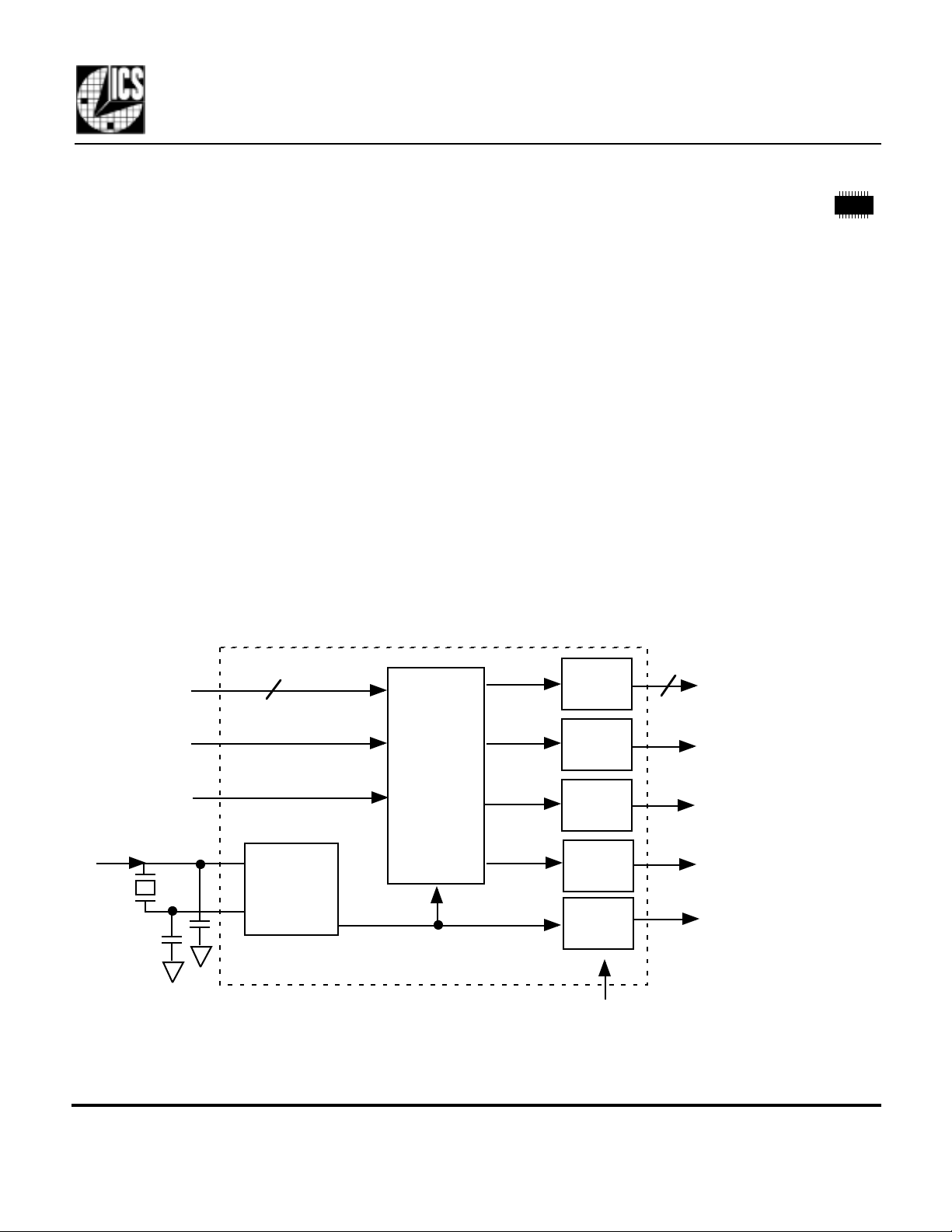
Block Diagram
Features
• Packaged in 20 pin tiny SSOP (QSOP)
• Operating VDD of 3.3V or 5V
• Less than one ppm synthesis error in all clocks
• Inexpensive 14.31818 MHz crystal or clock input
• Provides Ethernet and Fast Ethernet clocks
• Provides SCSI clocks
• Provides PCI clocks
• Selectable AC97 audio clock
• Selectable USB clock
• OE pin tri-states the outputs for testing
• Selectable frequencies on three clocks
• Duty cycle of 40/60
• Advanced, low power CMOS process
PSEL1:0
ASEL
USEL
14.31818 MHz
crystal
or clock
X1/ICLK
X2
2
Crystal
Oscillator
Clock
Synthesis
Circuitry
Output
Buffer
Output
Buffer
Output
Buffers
Output
Buffers
Output
Buffer
Output Enable (all outputs)
4
Processor Clocks
(Fast Ethernet,
SCSI, PCI )
Audio Clock
USB Clock
20 MHz
14.31818 MHz
MDS 650-01 C 1 Revision 092799 Printed 11/15/00
Integrated Circuit Systems • 525 Race Street • San Jose •CA•95126• (408) 295-9800tel • (408) 295-9818fax

ICS650-01
M
g
System Peripheral Clock Source
Pin Assignment
USEL
X2
X1/ICLK
VDD
VDD
GND
UCLK
20M
ACLK
PCLK4
1
2
3
4
5
6
7
8
9
10
20
19
18
17
16
15
14
13
12
11
PSEL1
PSEL0
PCLK2
PCLK3
VDD
ASEL
GND
14.318M
PCLK1
OE
Processor Clock (MHz)
PSEL1 PSEL0 PCLK1 PCLK2,3 PCLK4
0 0 25.00 50.00 18.75
0 M TEST TEST TEST
0 1 TEST TEST TEST
M 0 40.00 80.00 20.00
M M 33.3334 66.6667 25.00
M 1 20.00 40.00 25.00
1 0 20.00 33.3334 25.00
1 M 20.00 66.6667 25.00
1 1 Stops low all clocks except 20
Audio Clock (MHz)
ASEL ACLK
0 49.152
M 24.576
1 12.288
USB Clock (MHz)
USEL UCLK
012
M24
148
0 = connect directly to ground, 1 = connect directly
20 pin (150 mil) SSOP
to VDD, M=leave unconnected (floatin
)
Pin Descriptions
Pin # Name Type Description
1 USEL I UCLK Select pin. Determines frequency of USB clock per table above.
2 X2 XO Crystal connection. Connect to parallel mode 14.31818 MHz crystal. Leave open for clock.
3 X1/ICLK XI Crystal connection. Connect to parallel mode 14.31818 MHz crystal, or clock.
4 VDD P Connect to VDD. Must be same value as other VDD. Decouple with pin 6.
5 VDD P Connect to VDD. Must be same value as other VDD.
6 GND P Connect to ground.
7
8 20M O Fixed 20 MHz output for Ethernet. Only clock that runs when PSEL1=PSEL0=1.
9 ACLK O AC97 Audio clock output per table above.
10 PCLK4 O PCLK output number 4 per table above.
11 OE I Output Enable. Tri-states all outputs when low.
12 PCLK1 O PCLK output number 1 per table above.
13 14.318M O 14.31818 MHz buffered reference clock output.
14 GND P Connect to ground.
15 ASEL I ACLK Select pin. Determines frequency of Audio clock per table above.
16 VDD P Connect to VDD. Must be same value as other VDD. Decouple with pin 14.
17 PCLK3 O PCLK output number 3 per table above.
18 PCLK2 O PCLK output number 2 per table above.
19 PSEL0 I Processor Select pin #0. Determines frequencies on PCLKs 1-4 per table above.
20 PSEL1 I Processor Select pin #1. Determines frequencies on PCLKs 1-4 per table above.
UCLK O USB clock output per table above.
Key: I = Input; XO/XI = crystal connections; O = output; P = power supply connection
MDS 650-01 C 2 Revision 092799 Printed 11/15/00
Integrated Circuit Systems • 525 Race Street • San Jose •CA•95126• (408) 295-9800tel • (408) 295-9818fax
 Loading...