p
PRELIMINARY INFORMATION
HDTV Set-Top Clock Source
ICS627-01
Description
The ICS627-01 is a low cost, low jitter, high
performance clock synthesizer which can generate
frequencies required for HDTV receivers and settop boxes. Using ICS’s patented analog/digital
Phase-Locked Loop (PLL) techniques, the device
uses an inexpensive fundamental 27 MHz crystal
input to produce low jitter HDTV pixel clocks. It
has a separate input for a 1001/1000 or
2(1001/1000) conversion from a 13.5 MHz,
27 MHz or 54 MHz in
ut.
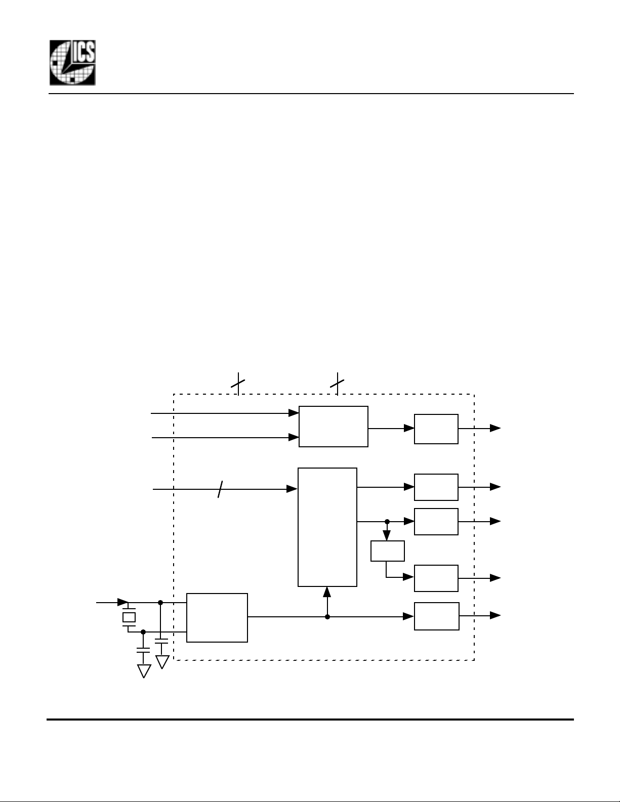
Block Diagram
VDD
Features
• Packaged in 28 pin SSOP (QSOP)
• HDTV frequencies of 74.25 and 74.175824 MHz
• Provides selectable B clock for 27.027 MHz or
other 1001/1000
• Uses a fundamental 27 MHz crystal or clock input
• All frequencies are generated exactly (zero ppm
synthesis error)
• Full CMOS output swings with 12 mA output
drive capability at TTL levels
• Advanced, low power, sub-micron CMOS process
• 3.3 V ±5% operating supply
GND
CLKIN
27.0 MHz
crystal or
clock
input
SB
SA2:0
X1/ICLK
X2
6
Crystal
Oscillator
x1001/1000
PLL
PLL
Clock
Synthesis
Circuitry
÷2
Output
Buffer
Output
Buffer
Output
Buffer
Output
Buffer
Output
Buffer
CLKB
CLKA
CLKC
(54 MHz)
CLKC/2
(27 MHz)
REFOUT
(27 MHz)
MDS 627-01 B 1 Revision 051600
Integrated Circuit Systems, Inc. • 525 Race Street • San Jose •CA•95126•(408) 295-9800tel • www.icst.com

PRELIMINARY INFORMATION
j
HDTV Set-Top Clock Source
ICS627-01
Pin Assignment
1
SA2
2
X2
3
X1
VDD
VDD
CLKIN
VDD
VDD
VDD
GND
GND
CLKC/2
CLKC
CLKB
4
5
6
7
8
9
10
11
12
13
14
28
27
26
25
24
23
22
21
20
19
18
17
16
15
SA2
SA0
SA0
REFOUT
GND
CLKA
VDD
GND
GND
GND
GND
SB
SA1
SA1
CLKA/CLKC Select Table (MHz)
SA2 SA1 SA0 Input CLKA CLKC CLKC/2
0 0 0 27.0 108.0 54.0 27.0
0 0 1 27.0 74.175824* TEST TEST
0 1 0 27.0 54.0 54.0 27.0
0 1 1 27.0 74.25* 54.0 27.0
1 0 0 TEST
1 0 1 27.0 74.175824 54.0 27.0
1 1 0 TEST
1 1 1 27.0 74.250 54.0 27.0
* These selections are recommended for the lowest
itter
CLKB Select Table (MHz)
SB CLKIN CLKB Multiplier
0 13.5 27.027 2002/1000
1 27 - 54 27.027 - 54.054 1001/1000
0 = connect directly to GND
1 = connect directl to VDD
Pin Descriptions
Number Name Type Description
1, 28 SA2 I Pins 1, 28 should be connected together. Selects CLKA and CLKC frequencies. Internal p-u.
2X2XOConnect to a fundamental 27.0 MHz crystal or leave unconnected for clock.
3 X1/ICLK XI Connect to a fundamental 27.0 MHz crystal or clock input.
4, 5, 7-9, 22 VDD P Connect to 3.3V.
6 CLKIN CI Clock input to produce 1001/1000 or 2(1001/1000) at CLKB. See table above.
10, 11, 18, 19 GND P Connect to ground.
12 CLKC/2 O C Clock output divided-by-2. See table above.
13 CLKC O C Clock output. See above table.
14 CLKB O B Clock output. See above table.
15, 16 SA1 I Pins 15, 16 should be connected together. Selects CLKA and CLKC frequencies. Internal p-u.
17 SB I B Clock Select. Selects CLKB frequency. See above table. Internal pull-up.
20, 21, 24 GND P Connect to ground.
23 CLKA O A Clock output. See above table.
25 REFOUT O 27 MHz Reference Output.
26, 27 SA0 I Pins 26, 27 should be connected together. Selects CLKA and CLKC frequencies. Internal p-u.
Key: I = Input; O = output; P = power supply connection; XI, XO = crystal connections; CI = clock input
MDS 627-01 B 2 Revision 051600
Integrated Circuit Systems, Inc. • 525 Race Street • San Jose •CA•95126•(408) 295-9800tel • www.icst.com
 Loading...