PRELIMINARY INFORMATION
ICS614-01
ICRO
C
LOCK
Description
The ICS614-01 is a low cost, low jitter, high
performance clock synthesizer for Intel’s i752
graphics systems. It includes frequencies for video
encoders and decoders. Using analog PhaseLocked Loop (PLL) techniques, the device accepts
a 27 MHz fundamental mode crystal or clock
input to produce multiple output clocks. The chip
provides highly accurate video encoder and
decoder clocks, as well as the 48 MHz necessary
for the Intel graphics processor, and can produce a
24.576 MHz audio clock.
See the ICS604 or ICS513 for 8 pin devices that
supply 48 MHz from a 14.31818 MHz input.
16 pin Intel Graphics Clock Source
Features
• Packaged in 16 pin SOIC
• Uses fundamental 27 MHz input crystal
• Supports Intel i752 graphics chip, popular video
encoders and decoders, and audio
• Low jitter - 50 ps one sigma
• Output Enable function tri-states outputs
• 25mA output drive capability at TTL levels
• Advanced, low power, sub-micron CMOS process
• 5V±10% core voltage. Inputs and outputs can run
3.3V (or 5V) for easy system interface
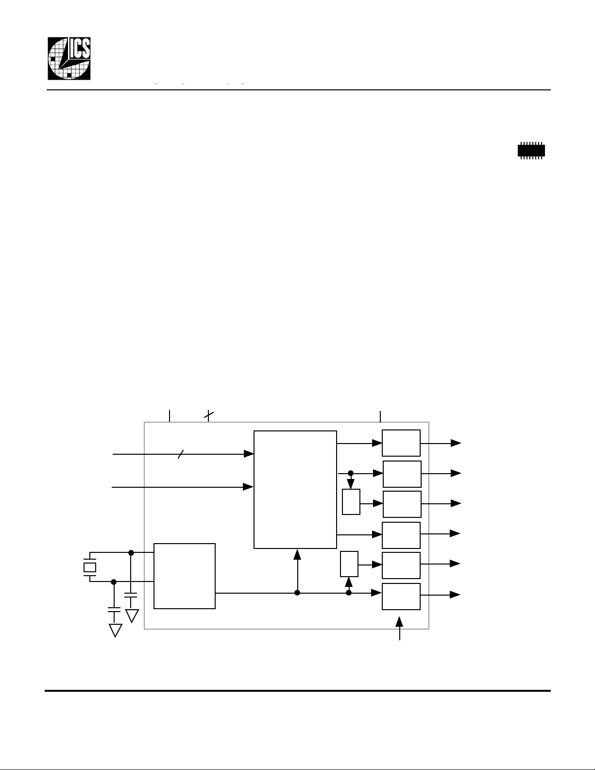
Block Diagram
ASEL1:0
DSEL
27 MHz crystal
X1
X2
VDD GND
2
Crystal
Oscillator
VDDIO
2
Clock Synthesis
and Control
Circuitry
Output
Buffer
Output
Buffer
÷2
÷2
Output
Buffer
Output
Buffer
Output
Buffer
Output
Buffer
Output Enable (all outputs)
ACLK
28.636 MHz or
35.4689 MHz
14.318 MHz or
17.7344 MHz
48 MHz
13.5 MHz
27 MHz
MDS 614-01 B 1 Revision 020199 Printed 11/14/00
Integrated Circuit Systems • 525 Race Street • San Jose •CA•95126• (408) 295-9800tel • (408) 295-9818fax

PRELIMINARY INFORMATION
ICS614-01
Pin Assignment
OE
X1/ICLK
VDD
GND
DSEL
27M
DCLK/2
X2
1
2
3
4
5
6
7
8
ICS614-01
ICRO
16
15
14
13
12
11
10
9
C
LOCK
ASEL1
ASEL0
13.5M
VDDIO
GND
ACLK
DCLK
48MHz
16 pin Intel Graphics Clock Source
ACLK Select Table for Audio and Square Pixel
ASEL1 ASEL0 ACLK
0 0 Off
0 1 29.4923 MHz
1 0 24.5454 MHz
1 1 24.576 MHz
DCLK Select Table for NTSC/PAL
DSEL DCLK DCLK/2
0 35.4689 17.73445
1 28.63636 14.31818
All Clock frequencies are in MHz.
0=connect directly to ground
1=connect directly to VDDIO
Pin Descriptions
Number Name Type Description
1 OE I Output Enable. Tri-states all output clocks when low. All running when high (VDDIO).
2 X2 XO Crystal connection. Connect to a 27 MHz fundamental parallel mode crystal.
3 X1/ICLK XI Crystal connection. Connect to a 27 MHz fundamental parallel mode crystal, or clock
4 VDD P Connect to +5V.
5 GND P Connect to ground.
6 DSEL I Input select. Determines DCLK and DCLK/2 per table above. Must be ≤ VDDIO.
7 27M O Buffered crystal oscillator 27 MHz clock output. Amplitude = VDDIO.
8 DCLK/2 O NTSC or PAL 4X subcarrier frequency per table above. Amplitude = VDDIO.
9 48M O 48.00 MHz clock output for Intel graphics processor. Amplitude = VDDIO.
10 DCLK O NTSC or PAL 8X subcarrier frequency per table above. Amplitude = VDDIO.
11 ACLK O Audio clock, or Square Pixel clock, per table above. Amplitude = VDDIO.
12 GND P Connect to ground.
13 VDDIO P Connect to +5V or +3.3V. Amplitude of output clocks will match this voltage.
14 13.5M O Buffered crystal oscillator divided by two 13.5 MHz clock output. Amplitude = VDDIO.
15 ASEL0 I Input select 0 for ACLK. Determines ACLK frequency per table above. Must be ≤ VDDIO.
16 ASEL1 I Input select 1 for ACLK. Determines ACLK frequency per table above. Must be ≤ VDDIO.
Key: I = Input; O = output; P = power supply connection; XI, XO = crystal connections.
MDS 614-01 B 2 Revision 020199 Printed 11/14/00
Integrated Circuit Systems • 525 Race Street • San Jose •CA•95126• (408) 295-9800tel • (408) 295-9818fax
 Loading...