PRELIMINARY
PRELIMINARY
INFORMATION
INFORMATION
Intel Graphics Clock Source
ICS604
Description
The ICS604 is the most cost effective way to
generate high quality, high frequency clocks for
Intel’s latest generation of graphics controllers. It
provides 48 MHz for the graphics controller, a
24.576 MHz clock for video or audio, as well as a
14.31818 MHz buffered output for the system
clock. Using patented Phase-Locked-Loop (PLL)
techniques, the ICS604 requires only a standard
fundamental mode, inexpensive crystal.
ICS makes additional devices to meet multiple
graphic system requirements. If the 24.576 MHz
clock is not needed, use the ICS513. If additional
frequencies are required for different video
encoders and decoders, see the ICS614-01.
Features
• Packaged as 8 pin SOIC or die
• Compatible with Intel graphics controllers
• Zero ppm synthesis error on 48 MHz output
• Input frequency of 14.31818 MHz
• Output clock frequencies of 48 MHz,
24.576 MHz, plus 14.31818 MHz Reference
output
• Low jitter
• Operating voltages of 3.0 to 5.5 V
• Full CMOS-level outputs with 25 mA drive
capability at TTL levels
• Advanced, low power CMOS process
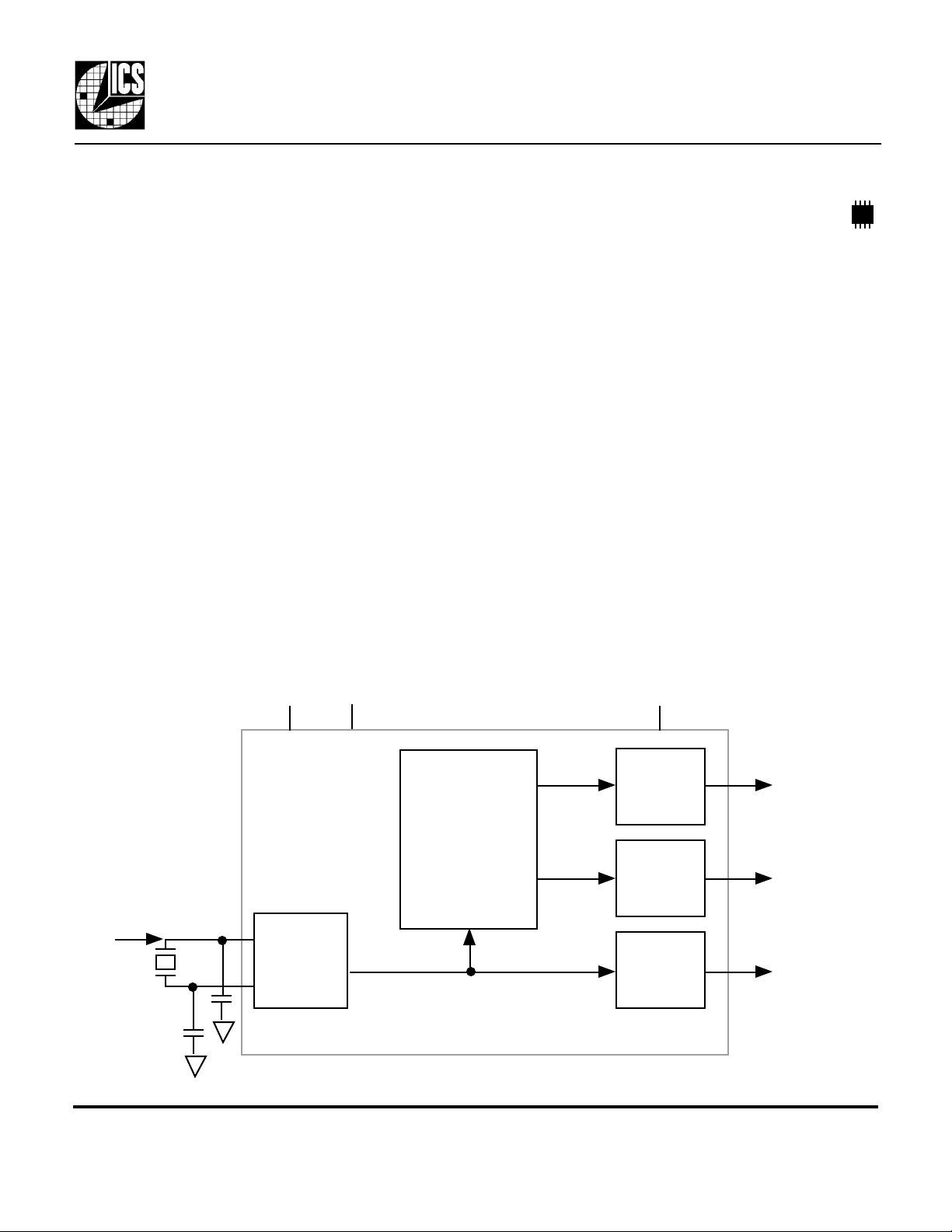
Block Diagram
14.318 MHz
crystal or clock
X1/ICLK
X2
VDDC GND
Crystal
Oscillator
PLL
Clock
Synthesis
and Control
Circuitry
VDDIO
Output
Buffer
Output
Buffer
Output
Buffer
48 MHz
24.576 MHz
14.318 MHz
MDS 604 A 1 Revision 022499 Printed 11/14/00
Integrated Circuit Systems • 525 Race Street • San Jose • CA • 95126 •(408)295-9800tel•(408)295-9818fax

Pin Assignment
PRELIMINARY
PRELIMINARY
INFORMATION
INFORMATION
Intel Graphics Clock Source
ICS604
X1/ICLK
VDDC
GND
14.3M
1 8
2
3
4
7
6
5
X2
VDDIO
24.576M
48M
Pin Descriptions
Number Name Type Description
1 X1/ICLK XI Crystal connection for 14.31818 MHz crystal, or clock input.
2 VDDC P Connect to +3.3V or +5V. +5 V recommended for lowest output noise (jitter).
3 GND P Connect to ground.
4 14.3M O Buffered crystal oscillator output clock.
5 48M O 48.0 MHz clock output for Intel graphics controller.
6 24.576M O 24.576 MHz clock output.
7 VDDIO P Connect to +3.3 V or +5 V. Cannot be greater than VDDC.
8 X2 XO Crystal connection for 14.31818 MHz crystal. Leave unconnected for clock input.
Key: I = Input; O = output; XI, XO = crystal connections; P = power supply connection
External Components / Crystal Selection
The ICS604 requires 0.01 µF decoupling capacitors to be connected between VDDC and GND, and
between VDDIO and GND. They must be connected close to the ICS604 to minimize lead inductance.
No external power supply filtering is required for this device. A 33 Ω terminating resistor can be used next
to the output pins when driving 50 Ω lines. The total on-chip crystal capacitance is approximately 6 pF,
and a parallel resonant, fundamental mode crystal should be used. Crystal capacitors should be connected
from each of the pins X1 and X2 to Ground as shown in the Block Diagram on page 1. The value (in pF)
of these crystal caps should be = (CL-6)*2, where CL is the crystal load capacitance in pF. For a clock
input, connect to X1 and leave X2 unconnected (no capacitors on either).
MDS 604 A 2 Revision 022499 Printed 11/14/00
Integrated Circuit Systems • 525 Race Street • San Jose • CA • 95126 •(408)295-9800tel•(408)295-9818fax
 Loading...