ICS601-01
Low Phase Noise Clock Multiplier
Description
The ICS601-01 is a low cost, low phase noise, high
performance clock synthesizer for any applications
that require low phase noise and low jitter. It is
ICS’ lowest phase noise multiplier, and also the
lowest CMOS part in the industry. Using ICS’
patented analog and digital Phase Locked Loop
(PLL) techniques, the chip accepts a 10-27 MHz
crystal or clock input, and produces output clocks
up to 156 MHz at 3.3 V.
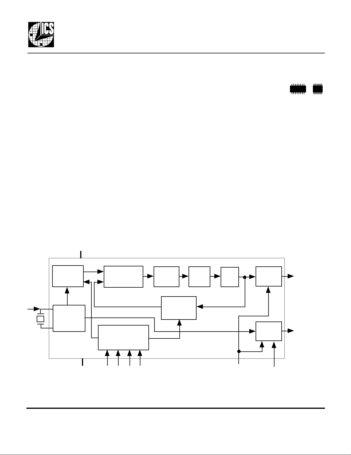
Block Diagram
Features
• Packaged in 16 pin SOIC or TSSOP
• Uses fundamental 10 - 27 MHz crystal, or clock
• Patented PLL with the lowest phase noise
• Output clocks up to 156 MHz at 3.3 V
• Low phase noise: -132 dBc/Hz at 10 kHz
• Output Enable function tri states outputs
• Low jitter - 18 ps one sigma
• Full swing CMOS outputs with 25 mA drive
capability at TTL levels
• Advanced, low power, sub-micron CMOS process
• Industrial temperature version available
• 3.3 V or 5 V operation
X1/ICLK
X2
VDD
Reference
Divide
Crystal
Oscillator
GND
Phase
Comparator
ROM Based
Multipliers
S3 S2
Charge
Pump
VCO
Divide
S0S1
Loop
Filter
VCO
OE
Output
Buffer
Output
Buffer
REFEN
CLK
REFOUT
MDS 601-01 G 1 Revision 090800 Printed 11/14/00
Integrated Circuit Systems, Inc. • 525 Race Street • San Jose •CA•95126• (408) 295-9800tel • www.icst.com

ICS601-01
Low Phase Noise Clock Multiplier
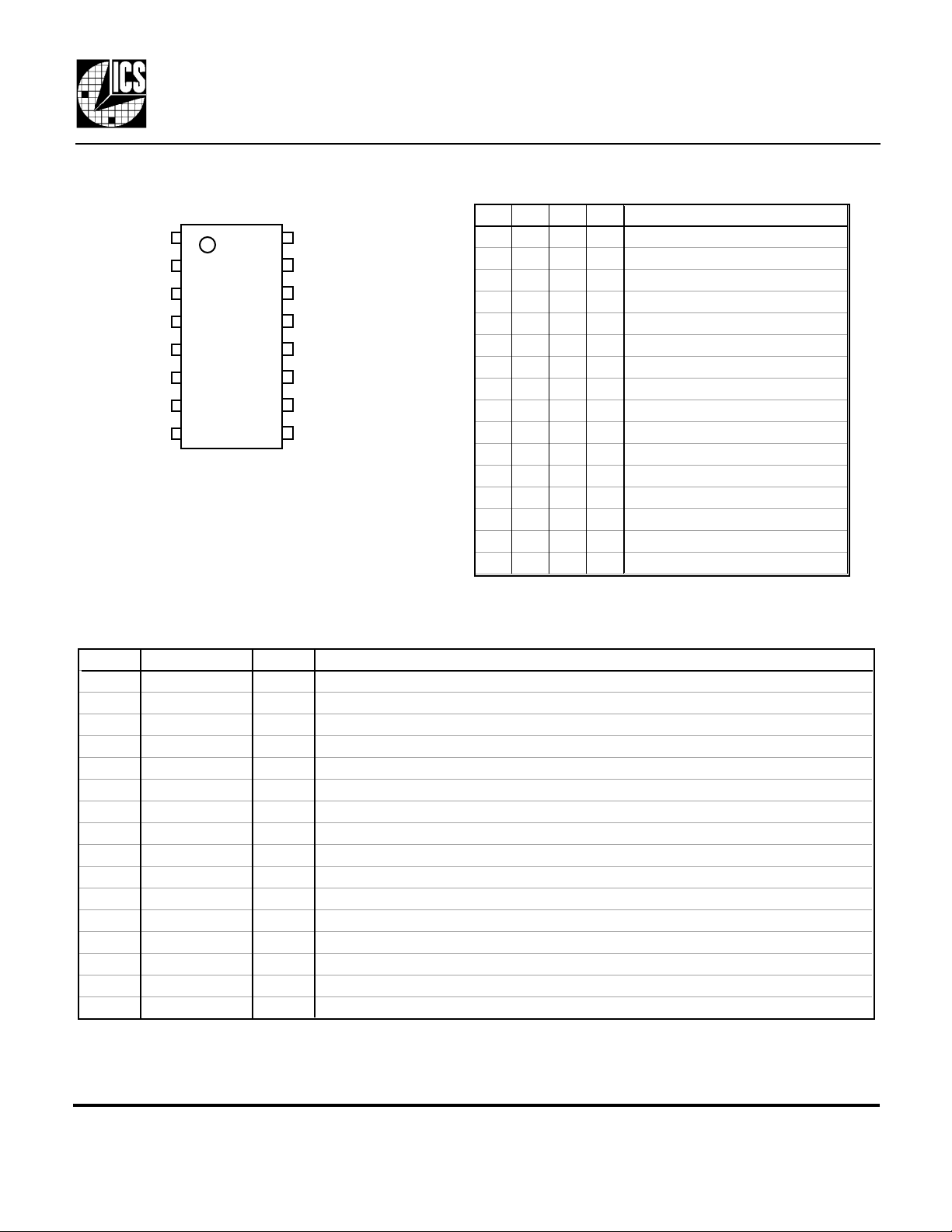
Pin Assignment
CLK
REFEN
VDD
VDD
VDD
X1/ICLK
X2
S1
1
2
3
4
5
6
7
8
ICS601-01
Pin Descriptions
16
15
14
13
12
11
10
9
GND
GND
GND
REFOUT
OE
S0
S3
S2
Multiplier Select Table
S3 S2 S1 S0 CLK (see note 2 on following page)
0 0 0 0 TEST
0 0 0 1 TEST
0 0 1 0 Input x1
0 0 1 1 Input x3
0 1 0 0 Input x4
0 1 0 1 Input x5
0 1 1 0 Input x6
0 1 1 1 Input x8
1 0 0 0 TEST
1 0 0 1 Crystal osc. pass through (no PLL)
1 0 1 0 Input x2
1 0 1 1 TEST
1 1 0 0 Input x8
1 1 0 1 Input x10
1 1 1 0 Input x12
1 1 1 1 Input x16
0=connect directly to ground
1=connect directly to VDD
Number Name Type Description
1 CLK O Clock output from VCO. Output frequency equals the input frequency times multiplier.
2 REFEN I Reference clock enable. Turns off the buffered crystal oscillator clock (stops low) when low.
3 VDD P Connect to +3.3V or +5V. Must match other VDDs.
4 VDD P Connect to +3.3V or +5V. Must match other VDDs.
5 VDD P Connect to +3.3V or +5V. Must match other VDDs.
6 X2 XO Crystal connection. Connect to a 10 - 27 MHz fundamental parallel mode crystal.
7 S1 I Multiplier select pin 1. Determines CLK output per table above. Internal pull-up.
8 X1/ICLK XI Crystal connection. Connect to a 10-27 MHz fundamental parallel mode crystal, or clock
9 S2 I Multiplier select pin 2. Determines CLK output per table above. Internal pull-up.
10 S3 I Multiplier select pin 3. Determines CLK output per table above. Internal pull-up.
11 S0 I Multiplier select pin 0. Determines CLK output per table above. Internal pull-up.
12 OE I Output Enable. Tri-states both output clocks when low. Internal pull-up.
13 REFOUT O Buffered crystal oscillator clock output. Controlled by REFEN.
14 GND P Connect to ground.
15 GND P Connect to ground.
16 GND P Connect to ground.
Key: I = Input with internal pull-up resistor; O = output; P = power supply connection; XI, XO = crystal
connections.
MDS 601-01 G 2 Revision 090800 Printed 11/14/00
Integrated Circuit Systems, Inc. • 525 Race Street • San Jose •CA•95126• (408) 295-9800tel • www.icst.com
 Loading...