Zero-Delay Glitch-Free Clock Multiplexer
Description Features
ICS581-01, -02
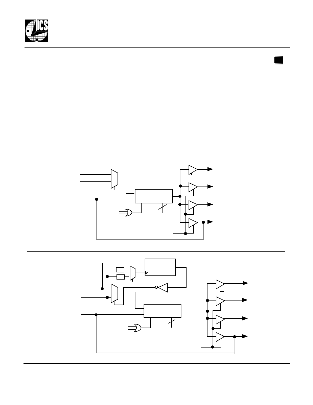
The ICS581-01 and ICS581-02 are glitch free,
Phase Locked Loop (PLL) based clock multiplexers
(mux) with zero delay from input to output. They
each have 4 low skew outputs which can be
configured as a single output, 3 outputs or 4
outputs. The ICS581-01 allows user control over
the mux switching. The ICS581-02 has automatic
switching between the 2 clock inputs.
The ICS581-01 and -02 are members of the ICS
Clock Blocks™ family of clock generation,
synchronization, and distribution devices. For a
non-PLL based clock mux, see the ICS580-01.
Block Diagrams
INA
INB
FBIN
ICS581-01
1
0
SELA
OE0
OE1
• Tiny 16 pin TSSOP package
• No short pulses or glitches on output. Operates to
200 MHz
• User controlled (ICS581-01) or automatic, timed
(ICS581-02) switch
• Low skew outputs
• Ideal for systems with backup or redundant clocks
• Zero delay, input to output
• 50% output duty cycle allows duty cycle correction
• Spread Smart™ technology works with spread
spectrum parts
CLK1
OE0
CLK2
PLL
2
S0, S1
OE1
CLK3
CLK4
External Feedback
NO_INA
CLK1
OE0
CLK2
CLK3
2
S0, S1
CLK4
OE1
ICS581-02
INA
INB
FBIN
1
0
÷48
÷3
OE0
OE1
1
0
DIV
IN
Transition
Detector
PLL
External Feedback
MDS 581-01, 581-02 A 1 Revision 041100 Printed 11/14/00
Integrated Circuit Systems, Inc. • 525 Race Street • San Jose •CA•95126• (408) 295-9800tel • www.icst.com

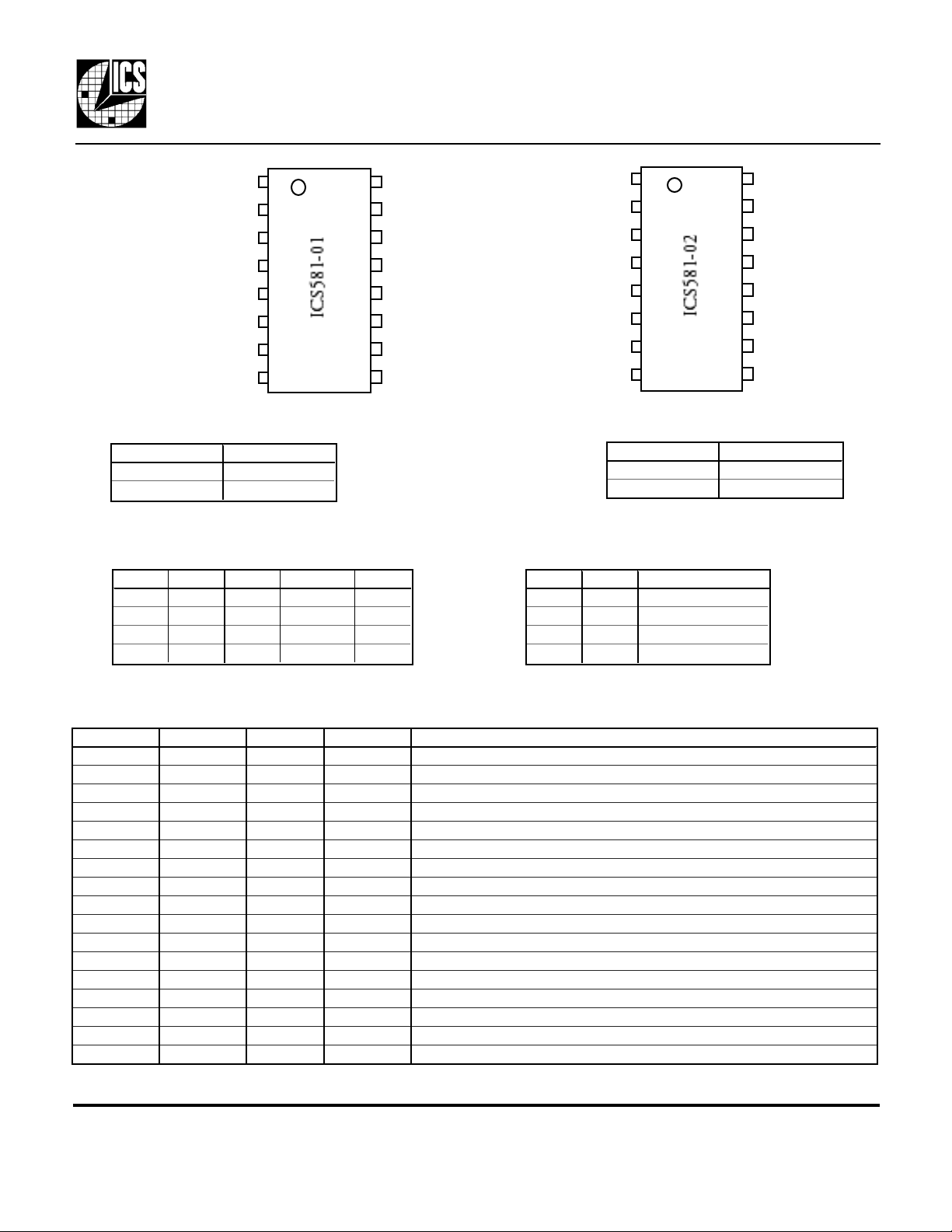
Pin Assignment
S0
S1
VDD
INA
INB
GND
FBIN
OE0
ICS581-01, -02
Zero-Delay Glitch-Free Clock Multiplexer
1
2
3
4
5
6
7
8
16
15
14
13
12
11
10
SELA
VDD
CLK1
CLK2
CLK3
CLK4
GND
9
OE1
S0
S1
VDD
INA
INB
GND
FBIN
OE0
1
2
3
4
5
6
7
8
16
15
14
13
12
11
10
DIV
VDD
CLK1
CLK2
CLK3
CLK4
GND
9
OE1
Clock Decoding
SELA CLK1:4
0 INB
1 INA
ICS581-01 only
Tri-State and Power Down
OE1 OE0 CLK1 CLK2,3,4 PLL
0 0 Z Z Off
0 1 On Z On
1 0 Z On On
1 1 On On On
ICS581-01,-02
Frequency Range Select
S1 S0 Input Range (MHz)
0 0 50-150
0 1 19-75
1 0 6-19
1 1 150-200
ICS581-01,-02
Timeout Selection
DIV Nominal Timeout
0 3xPeriod of INB
1 48xPeriod of INB
ICS581-02 only
Pin Descriptions
Number Name Type Chip Description
1 S0 I -01, -02 Select 0 for frequency range. See table. Internal pull-up.
2 S1 I -01, -02 Select 1 for frequency range. See table. Internal pull-up.
3 VDD P -01, -02 Connect to +3.3 V or + 5 V.
4 INA I -01, -02 Input Clock A.
5 INB I -01, -02 Input Clock B.
6 GND P -01, -02 Connect to ground.
7 FBIN I -01, -02 Feedback input. Connect to a clock output.
8 OE0 I -01, -02 Output Enable0. See Table. Internal pull-up.
9 OE1 I -01, -02 Output Enable1. See Table. Internal pull-up.
10 GND P -01, -02 Connect to ground.
11 CLK4 O -01, -02 Low skew clock output.
12 CLK3 O -01, -02 Low skew clock output.
13 CLK2 O -01, -02 Low skew clock output.
14 CLK1 O -01, -02 Low skew clock output.
15 VDD P -01, -02 Connect to +3.3 V or + 5 V.
16 SELA I -01 only Mux select. Selects INA when high. Internal pull-up.
16 DIV I -02 only Timeout select. See table. Internal pull-up.
Key: I = Input; O = output; P = power supply connection
MDS 581-01, 581-02 A 2 Revision 041100 Printed 11/14/00
Integrated Circuit Systems, Inc. • 525 Race Street • San Jose •CA•95126• (408) 295-9800tel • www.icst.com
 Loading...