ICS580-01
Glitch-Free Clock Multiplexer
Description
The ICS580-01 is a clock multiplexer (mux)
designed to switch between 2 clock sources with no
glitches or short pulses. The operation of the mux is
controlled by an input pin but the part can also be
configured to switch automatically if one of the
input clocks stops. The part also provides clock
detection by reporting when an input clock has
stopped.
For a clock mux with zero delay and smooth
switching, see either the ICS581-01 or ICS581-02.
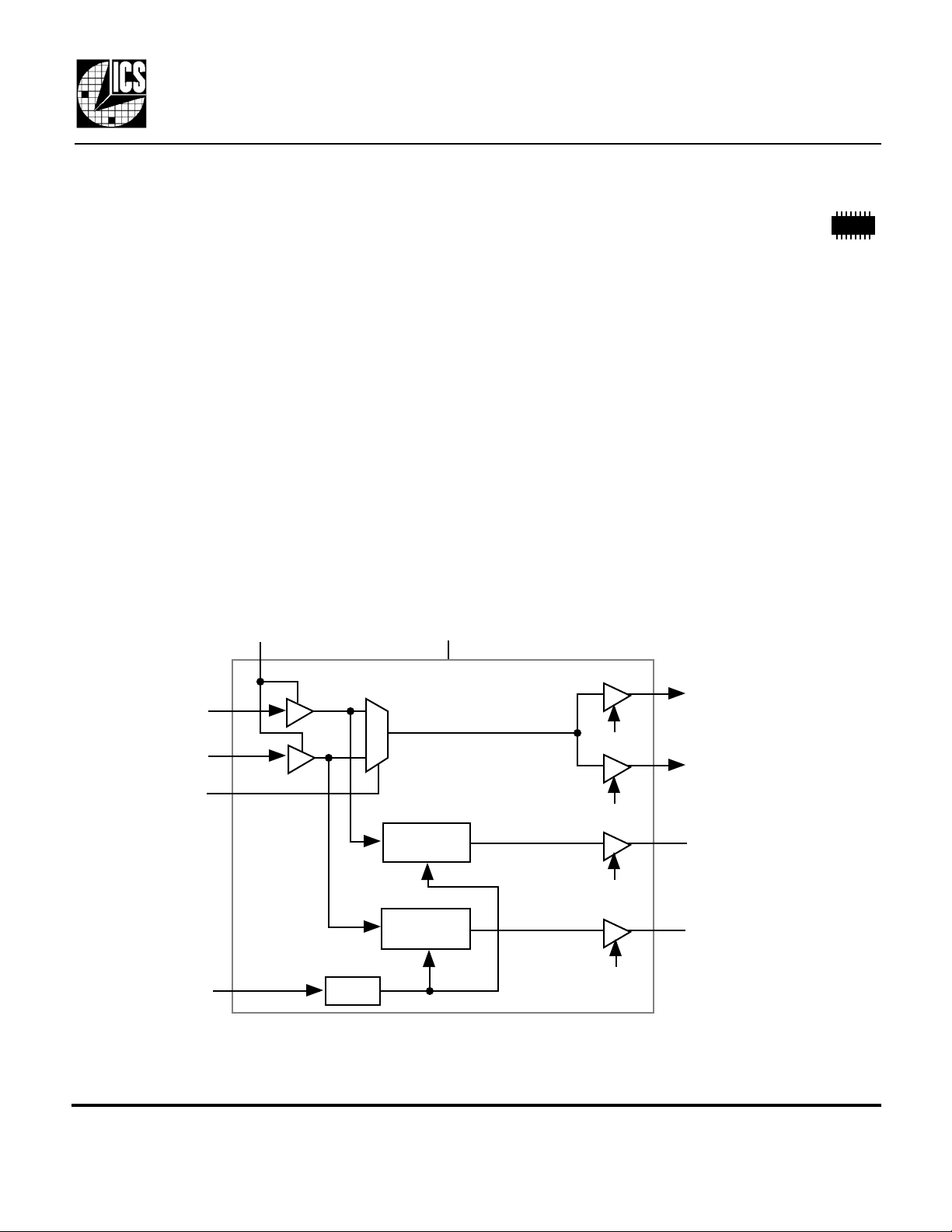
Block Diagram
VDDI
VDDC
Features
• Packaged in 16 pin narrow (150 mil) SOIC
• No short pulses or glitches on output
• Operates to 200 MHz
• Does not add jitter or phase noise to the clock
• User controlled or automatic switching
• Low skew outputs
• Clock detect feature
• Ideal for systems with backup or redundant clocks
• Selectable timeouts for clock detection
• Separate supply voltages allow power supply voltage
translation
• Operates to 2.5 V
CLK1
INB
INA
SELB
DIV
MDS 580-01 A 1 Revision 030300 Printed 11/28/00
Timer
1
0
Transition
Detector
Transition
Detector
OE1
CLK2
OE2
NO_INA
OE3
NO_INB
OE4
Integrated Circuit Systems, Inc. • 525 Race Street • San Jose •CA•95126• (408) 295-9800tel • www.icst.com

Pin Assignment
ICS580-01
Glitch-Free Clock Multiplexer
SELB
DIV
VDDI
INA
INB
GND
OE4
OE3
1
16
2
3
4
5
6
7
8
1415CLK1
13
12
11
10
9
Pin Descriptions
Number Name Type Description
1 SELB I Mux select. Selects INB when high. Internal pull-up.
2 DIV I Time out select. See table above. Internal pull-up.
3 VDDI P Supply for input clocks only. Can be higher than VDDC.
4 INA I Input Clock A.
5 INB I Input Clock B.
6 GND P Connect to ground.
7 OE4 I Output Enable. Tri-states NO_INB when low. Internal pull-up.
8 OE3 I Output Enable Tri-states NO_INA when low. Internal pull-up.
9 OE2 I Output enable. Tri-states CLK2 when low. Internal pull-up.
10 GND P Connect to ground.
11 NO_INB O Goes high when clock on INB stops.
12 NO_INA O Goes high when clock on INA stops.
13 CLK2 O Clock 2 Output. Low skew compared to CLK1.
14 CLK1 O Clock 1 Output. Low skew compared to CLK2.
15 VDDC P Main chip supply. Output clocks amplitude will match this VDD.
16 OE1 I Output Enable. Tri-states CLK1 when low. Internal pull-up.
OE1
VDDC
CLK2
NO_INA
NO_INB
GND
OE2
Timeout Selection
DIV Nominal Timeout
0 600 ns
1 75 ns
Key: I = Input; O = output; P = power supply connection
MDS 580-01 A 2 Revision 030300 Printed 11/28/00
Integrated Circuit Systems, Inc. • 525 Race Street • San Jose •CA•95126• (408) 295-9800tel • www.icst.com
 Loading...