Zero Delay, Low Skew Buffer
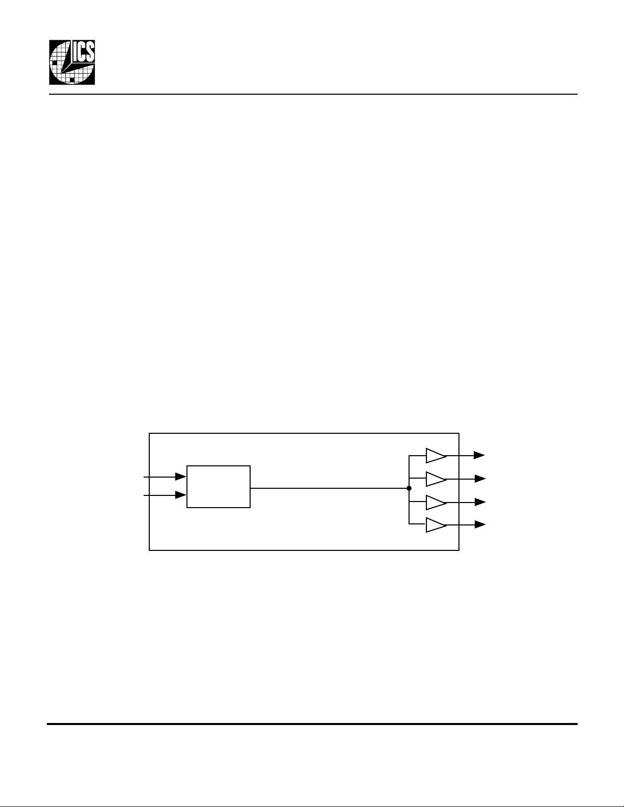
PLL-based zero delay buffer for high speed
applications. Based on ICS’s proprietary low jitter
Phase Locked Loop (PLL) techniques, the device
provides four low skew outputs at speeds up to 160
MHz at 3.3 V. When one of the outputs is connected
directly to FBIN, the rising edge of each output is
aligned with the rising edge of the input clock. External
delay elements connected in the feedback loops will
cause the outputs to occur before the inputs by the
amount of propagation delay of the external element.
ICS manufactures the largest variety of clock
generators and buffers, and is the largest clock
supplier in the world.
Description Features
ICS574
The ICS574 is a low jitter, low-skew, high performance
Block Diagram
• Packaged in 8 pin narrow SOIC
• Zero input-to-output delay
• Four 1X outputs
• Output to output skew is less than 150 ps
• Output clocks up to 160 MHz at 3.3 V
• External feedback path for output edge placement
• Spread Smart™ technology works with spread
spectrum clock generators
• Full CMOS outputs with 18 mA output drive
capability at TTL levels at 3.3 V
• Advanced, low power, sub-micron CMOS process
• Operating voltage from 3.0 to 5.5 V
FBIN
CLKIN
MDS 574 B 1 Revision 051801
Integrated Circuit Systems, Inc. • 525 Race Street • San Jose • CA • 95126 • (408)295-9800 • www.icst.com
PLL
CLK1
CLK2
CLK3
CLK4

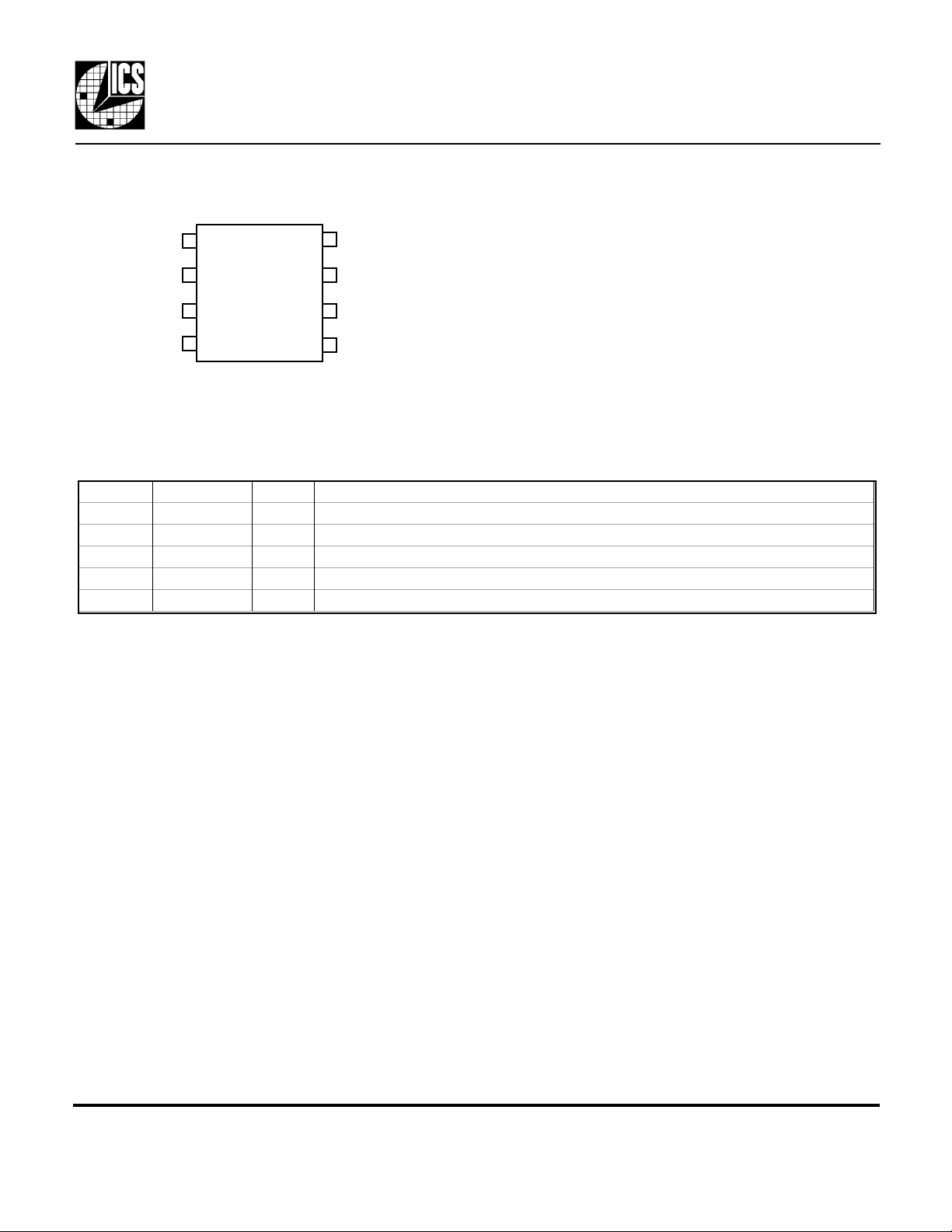
Pin Assignment
ICS574
Zero Delay, Low Skew Buffer
CLKIN
CLK1
CLK2
GND
1 8
2
3
4
Standard 8 pin SOIC
FBIN
7
CLK4
6
CLK3
5
VDD
Pin Descriptions
Number Name Type Description
1 CLKIN I Clock input. Connect to input clock source.
2, 3, 6, 7 CLK1:4 O Four clock outputs.
5 VDD P Power supply. Connect both pins to same voltage (either 3.3V or 5V).
4 GND P Connect to ground.
8 FBIN I Feedback input.
Key: I = Input; O = output; P = power supply connection.
External Components
The ICS574 requires a minimum number of external components for proper operation. Decoupling capacitors of
0.1µF should be connected between VDD and GND on pins 4 and 5, as close to the device as possible. A series
termination resistor of 33 Ω may be used close to the pin for each clock output to reduce reflections.
MDS 574 B 2 Revision 051801
Integrated Circuit Systems, Inc. • 525 Race Street • San Jose • CA • 95126 • (408)295-9800 • www.icst.com
 Loading...