ICS570A
Multiplier and Zero Delay Buffer
Description
The ICS570A is a high performance Zero Delay
Buffer (ZDB) which integrates ICS’ proprietary
analog/digital Phase Locked Loop (PLL) techniques.
ICS introduced the world standard for these devices
in 1992 with the debut of the AV9170. The
ICS570A, part of ICS’ ClockBlocks™ family, was
designed as a performance upgrade to meet today’s
higher speed and lower voltage requirements. The
zero delay feature means that the rising edge of the
input clock aligns with the rising edges of both
outputs, giving the appearance of no delay through
the device. There are two outputs on the chip, one
being a low-skew divide by two of the other. The chip
has an all-chip power down/tri-state mode that stops
the internal PLL and puts both outputs into the high
impedance state.
The chip is ideal for synchronizing outputs in a large
variety of systems, from personal computers to data
communications to video. By allowing off-chip
feedback paths, the ICS570A can eliminate the delay
through other devices.
The ICS570A was done to improve jitter from the
original ICS570, and so it is recommended for all new
designs.
Features
• Packaged in 8 pin SOIC.
• Pin-for-pin replacement and upgrade to ICS570
• Functional equivalent to AV9170 (not a pin for-pin replacement).
• Low input to output skew of 500 ps max.
• Low skew (250 ps) outputs. One is ÷ 2 of other.
• Ability to choose between 14 different
multipliers from 0.5X to 32X.
• Input clock frequency up to 150 MHz at 3.3V.
• Can recover poor input clock duty cycle.
• Output clock duty cycle of 45/55.
• Power Down and Tri-State Mode.
• Full CMOS clock swings with 25mA drive
capability at TTL levels.
• Advanced, low power CMOS process.
• Operating voltage of 3.0 to 5.5 V.
• Industrial temperature version available
Block Diagram
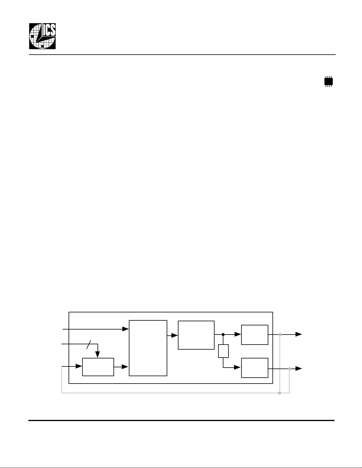
ICLK
S1, S0
FBIN
MDS 570A C 1 Revision 102700 Printed 11/14/00
Integrated Circuit Systems, Inc .• 525 Race Street • San Jose • CA •95126• (408)295-9800tel •www.icst.com
2
divide by
N
External feedback can come from CLK or CLK/2 (see table on page 2).
Phase
Detector,
Charge
Pump, and
Loop Filter
Voltage
Controlled
Oscillator
÷2
Output
Buffer
Output
Buffer
CLK
CLK/2

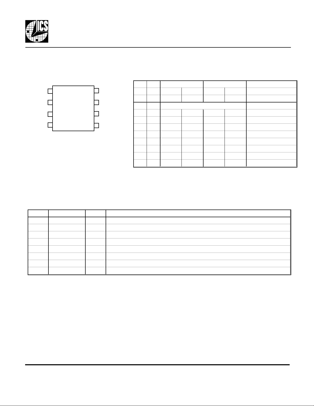
Pin Assignment
FBIN from CLK
FBIN from CLK/2
Power Down and Tri-State
1 8
S1
VDD
GND
ICLK
2
3
4
8 pin SOIC
7
6
5
CLK/2
CLK
S0
FBIN
ICS570A
Multiplier and Zero Delay Buffer
Clock Multiplier Decoding Table
(Multiplies input clock by shown amount)
ICLK Input Range
S1 S0 CLK CLK/2 CLK CLK/2 FB from CLK/2 *
#1 #6 pin # 7 pin # 8 pin # 7 pin # 8 (3.3V, MHz)
0 0
0 M x3 x1.5 x6 x3 2.5 to 25
0 1 x4 x2 x8 x4 2.5 to 19
M 0 x8 x4 x16 x8 2.5 to 9.5
M M x6 x3 x12 x6 2.5 to 12.5
M 1 x10 x5 x20 x10 2.5 to 7.5
1 0 x1 ÷2 x2 x1 5 to 75
1 M x16 x8 x32 x16 2.5 to 5
1 1 x2 x1 x4 x2 2.5 to 37.5
0 = connect directly to ground.
M = leave unconnected (self-biases to VDD/2).
1 = connect directly to VDD.
*Input range with CLK feedback is double that for CLK/2.
-
Pin Descriptions
Number Name Type Description
1 S1 I Select 1 for output clock. Connect to GND, VDD, or float per decoding table above.
2 VDD P Connect to +3.3V or +5V.
3 GND P Connect to ground.
4 ICLK CI Reference clock input.
5 FBIN CI Feedback clock input.
6 S0 I Select 0 for output clock. Connect to GND, VDD, or float per decoding table above.
7 CLK O Clock output per Table above.
8 CLK/2 O Clock output per Table above. Low skew divide by two of pin 7 clock.
Key: CI = clock input, I = input, O = output, P = power supply connection
External Components
The ICS570A requires a 0.01 µF decoupling capacitor to be connected between VDD and GND. It must
be connected close to the ICS570A to minimize lead inductance. No external power supply filtering is
required for this device. A 27 Ω terminating resistor can be used next to each output pin.
MDS 570A C 2 Revision 102700 Printed 11/14/00
Integrated Circuit Systems, Inc .• 525 Race Street • San Jose • CA •95126• (408)295-9800tel •www.icst.com
 Loading...