PRELIMINARY INFORMATION
ICS554-01
LOW SKEW 1 TO 4 CLOCK BUFFER PECL IN, PECL OUT
Description
The ICS554-01 is a low skew clock buffer with a single
complimentary PECL input to four PECL outputs. Part
of ICS’ Clock Blocks
PECL clock buffer. For parts which do not require PECL
inputs or outputs, see the ICS553 for a 1 to 4 low skew
buffer, or the ICS552-02 for a 1 to 8 low skew buffer. For
more than 8 outputs see the MK74CBxxx Buffalo
series of clock drivers.
ICS makes many non-PLL and PLL based low skew
output devices as well as Zero Delay Buffers to
synchronize clocks. Contact us for all of your clocking
needs.
TM
family, this is our lowest skew
TM
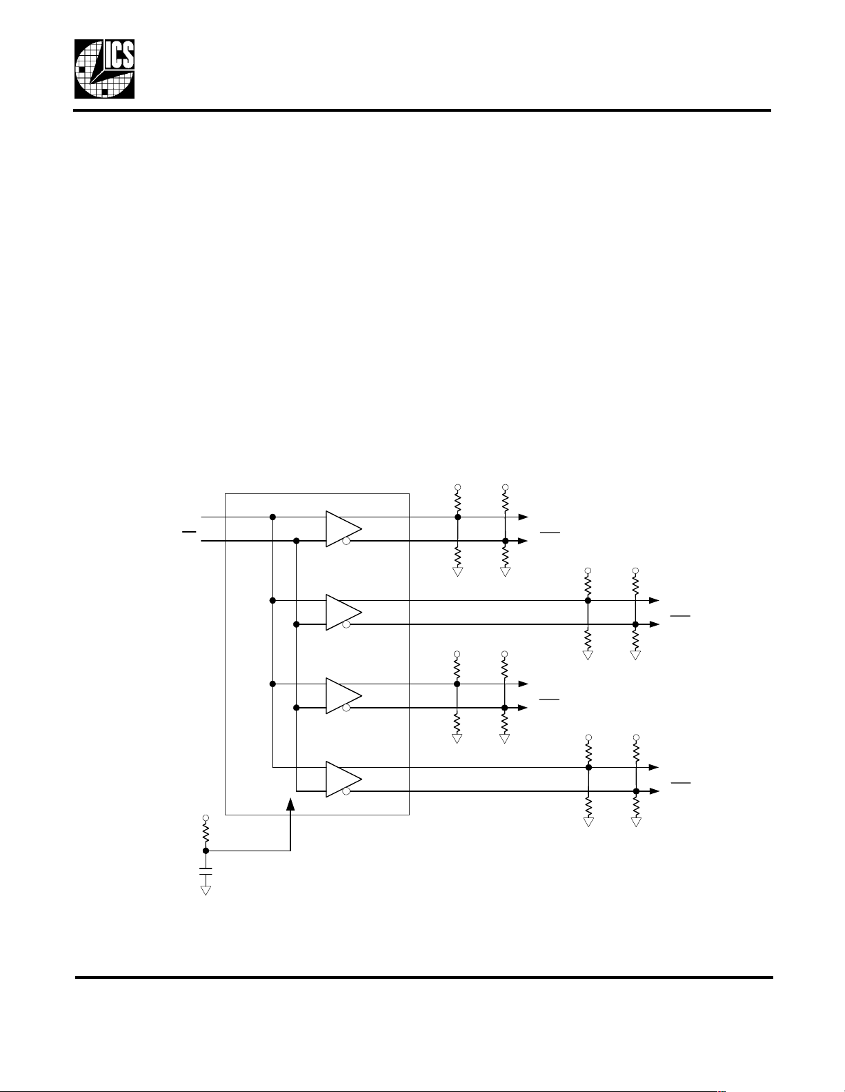
Block Diagram
IN
IN
Features
• Outputs are skew matched to within 50ps
• Packaged in 16 pin TSSOP
• One PECL input to 4 PECL output clock drivers
• Operating Voltages of 3.3V to 5V
VDD
62Ω 62Ω
Q0
270Ω 270Ω
Q0
VDD
62Ω 62Ω
Q1
Q1
VDD
62Ω 62Ω
270Ω 270Ω
Q2
270Ω 270Ω
Q2
VDD
62Ω 62Ω
Q3
VDD
1.1kΩ
0.01mF
MDS 554-01 A 1 Revision 031901
Integrated Circuit Systems ● 525 Race Street, San Jose, CA 95126 ● tel (408) 295-9800 ● www.icst.com
RES
270Ω 270Ω
Q3

PRELIMINARY INFORMATION ICS554-01
12
1
11
2
10
3
9
NC
4
VDD
5
6
VDD
7
Q0
8
Q3
Q3
Q2
Q1
IN
GND GND
16
15
14
13
IN
RES
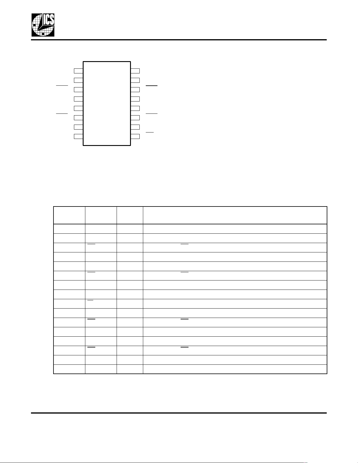
16 Pin TSSOP
Q0
Q1
Q2
Pin Assignment
LOW SKEW 1 TO 4 CLOCK BUFFER PECL IN, PECL OUT
Pin Descriptions
Pin
Number
1 NC - No Connect.
2 VDD Power Connect to +2.5 V, +3.3V or +5.0V. Must be the same as pin 15.
3Q0
4 Q0 Output Clock Output Q0
5 Q1 Output Clock Output Q1
6Q1
7 GND Power Ground
8 IN Input PECL Clock Input
9IN
10 GND Power Ground
11 Q2
12 Q2 Output Clock Output Q2
13 Q3 Output Clock Output Q3
14 Q3
15 VDD Power Connect to +2.5V, +3.3V or +5.0V. Must be the same as pin 2
MDS 554-01 A 2 Revision 031901
Integrated Circuit Systems ● 525 Race Street, San Jose, CA 95126 ● tel (408) 295-9800 ● www.icst.com
16 RES Input Bias Resistor Input.
Pin
Name
Output Clock Output Q0
Output Clock Output Q1
Output Clock Output Q2
Output Clock Output Q3
Pin
Typ e
Input Complementary PECL Clock Input
Pin Description
 Loading...