ICST ICS552R-01, ICS552R-01I, ICS552R-01IT, ICS552R-01T Datasheet

ICS552-01A
Crystal Oscillator & Multiplier with 8 Low Skew Outputs
Description
The ICS552-01A produces 8 low skew
copies of a multiple of the input when a
clock or fundamental, parallel-mode crystal
is connected to it. Unlike other clock
drivers, it does not require a separate
oscillator for the input. Using a phaselocked loop (PLL) to multiply the input
frequency, it is ideal for generating and
distributing multiple high frequency clocks.
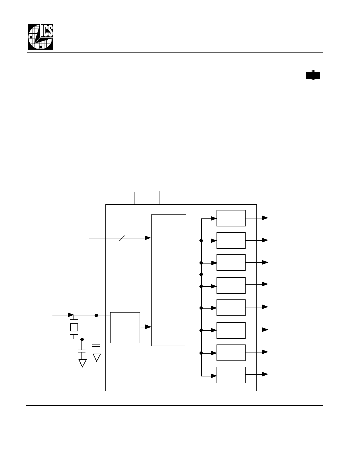
Block Diagram
VDD GND
Features
• Packaged in 20 pin SSOP (QSOP)
• Input frequency of 10.0 - 27.0 MHz
• Contains on-chip multiplier with selections
of x1, x1.33, x2, x2.66, x3, x3.33, x4,
x4.66, x5, and x6
• Provides 8 low skew outputs (<250 ps)
• Output clock duty cycle of 40/60 at 3.3 V
• Operating voltages of 3.0 V to 5.5 V
• Industrial temperature available
• Power Down and Tri state modes
Output
Buffer
CLK1
10.0 - 27.0 MHz
crystal or clock
S3:S0
X1
X2
4
Clock
Buffer/
Crystal
Oscillator
PLL
Multiplier
Output
Buffer
Output
Buffer
Output
Buffer
Output
Buffer
Output
Buffer
Output
Buffer
Output
Buffer
CLK2
CLK3
CLK4
CLK5
CLK6
CLK7
CLK8
MDS 552-01 AB 1 Revision 032200 Printed 11/14/00
Integrated Circuit Systems • 525 Race Street • San Jose • CA • 95126 • (408) 295-9800tel • www.icst.com

Pin Assignment
S2
1
2
3
4
5
6
7
8
9
10
DC
X2
X1/ICLK
VDD
GND
CLK1
CLK2
CLK3
CLK4
20 pin SSOP (QSOP)
ICS552-01A
Crystal Oscillator & Multiplier with 8 Low Skew Outputs
Multiplier Select Table
S0
20
19
18
17
16
15
14
13
12
11
DC
CLK8
CLK7
VDD
S3
GND
CLK6
CLK5
S1
S3 S2 S1 S0 Multiplier
0 0 0 0 Power Down
0 0 0 1 x1
0 0 1 0 x1.333
0 0 1 1 x2
0 1 0 0 x2.666
0 1 0 1 x3
0 1 1 0 x3.333
0 1 1 1 x4
1 0 0 0 x5
1 0 0 1 x4.66
1 0 1 0 x6
1 1 0 1 Tri state All
0 = connect directly to ground.
1 = connect directly to VDD.
All clocks stop low in Power Down state.
All clocks outputs are high impedance in 1101 mode.
Pin Descriptions
Pin # Name Type Description
1 DC - Don't connect.
2 X2 XO Crystal connection. Connect to a 10 - 27 MHz fundamental mode crystal.
3 X1/ICLK XI Crystal connection. Connect to a 10 - 27 MHz fundamental mode crystal, or clock.
4 VDD P Connect to +3.3 V or +5.0 V. Decouple with pin 6.
5 S2 I Multiplier Select Pin 2 per table above.
6 GND P Connect to ground.
7
8 CLK2 O Clock Output 2.
9 CLK3 O Clock Output 3.
10 CLK4 O Clock Output 4.
11 S1 I Multiplier Select Pin 1 per table above.
12 CLK5 O Clock Output 5.
13 CLK6 O Clock Output 6.
14 GND P Connect to ground.
15 S3 I Multiplier Select Pin 3 per table above.
16 VDD P Connect to +3.3 V or +5.0 V. Decouple with pin 14.
17 CLK7 O Clock Output 7.
18 CLK8 O Clock Output 8.
19 DC - Don't connect.
20 S0 I Multiplier Select Pin 0 per table above.
CLK1 O Clock Output 1.
Key: I = Input; O = output; P = power supply connection, XI, XO = crystal connections
MDS 552-01 AB 2 Revision 032200 Printed 11/14/00
Integrated Circuit Systems • 525 Race Street • San Jose • CA • 95126 • (408) 295-9800tel • www.icst.com
 Loading...