ICS552-03
LOW SKEW 1 TO 8 CLOCK BUFFER (4 AT 1X, 4 AT 1/2X)
Description
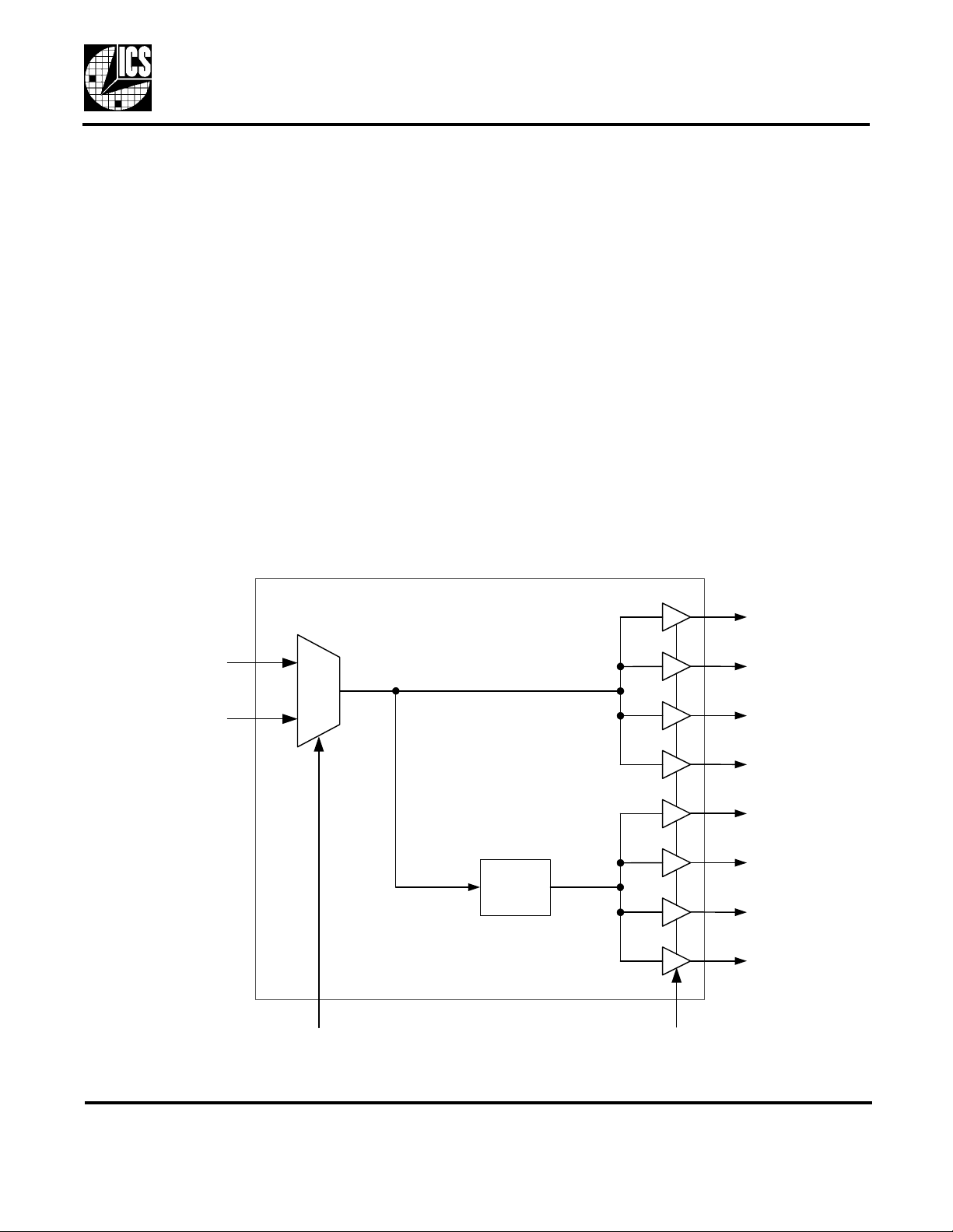
The ICS552-03 is a low skew, single input to eight
output clock buffer. Four of the outputs are exact copies
of the input, while the other four are divide by 2 copies
of the input. It is part of ICS’ Clock Blocks
the ICS553 for a 1 to 4 low skew buffer , or the
ICS552-02 for a 1 to 8 low skew buffer without divide by
2. For more than 8 outputs see the MK74CBxxx
Buffalo
ICS makes many non-PLL and PLL based low skew
output devices as well as Z ero Delay Buffers to
synchronize clocks. Contact us for all of your clocking
needs.
TM
series of cloc k drivers.
TM
family. See
Block Diagram
Features
• Low skew outputs (50 ps maximum)
• Packaged in 16 pin TSSOP
• Low power CMOS technology
• Operating Voltages of 2.5 V to 5 V
• Output Enable pin tri-states outputs
• Low skew between 1X and 1/2X outputs (100 ps
maximum)
• One bank of 4 outputs at 1X
• One bank of 4 outputs at 1/2X
• 5V tolerant input clocks
• Input clock multiplexer
Q0
IN A
IN B
1
0
SELA
Q1
Q2
Q3
P0
P1
Divide
by 2
P2
P3
OE
MDS 552-03 B 1 Revision 052501
Integrated Circuit Systems ● 525 Race Street, San Jose, CA 95 126 ● tel (408) 295-9800 ● www.icst.com

LOW SKEW 1 TO 8 CLOCK BUFFER (4 AT 1X, 4 AT 1/2X)
Pin Assignment Input Source Select
ICS552-03
OE
VDD
Q0
Q1
Q2
Q3
GND GND
INB
1
2
3
4
5
6
7
8
16 Pin 173 Mil (0.65mm) TSSOP
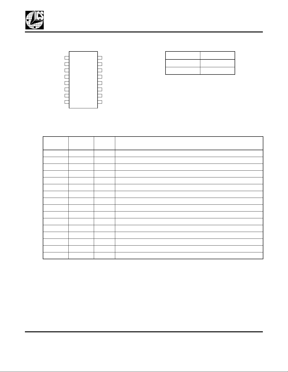
Pin Descriptions
Pin
Number
1 OE Input Output Enable. Tri-states outputs when low.Internal Pull-up resistor
2 VDD Power Connect to +2.5 V, +3.3 V or +5.0 V. Must be the same as pin 15
3 Q0 Output Clock Output Q0
4 Q1 Output Clock Output Q1
5 Q2 Output Clock Output Q2
6 Q3 Output Clock Output Q3
7 GND Power Ground
8 INB Input Clock Input B. 5 V tolerant input
9 INA Input Clock Input A. 5 V tolerant input
10 GND Power Ground
11 P0 Output Clock Output P0
12 P1 Output Clock Output P1
13 P2 Output Clock Output P2
14 P3 Output Clock Output P3
15 VDD Power Connect to +2.5 V, +3.3 V or +5.0 V. Must be the same as pin 2
16 SELA Input Selects either INA or INB. Internal pull-up resistor
Pin
Name
16
15
14
13
12
11
10
9
SELA
VDD
P3
P2
P1
P0
INA
Pin
Type
SELA Input
0INB
1INA
Pin Description
External Components
A minimum number of external components are required for proper operation. Decoupling capacitors of
0.01 µF should be connected between VDD on pin 2 and GND on pin 7,and between VDD on pin 15 and
GND on pin 10, as close to the device as possible. A 33 Ω series terminating resistor should be used on
each clock output if the trace is longer than 1 inch.
To achieve the low output skews that the ICS552-03 is capable of, careful attention must be paid to board
layout. Essentially, all 8 outputs must have identical terminations, identical loads, and identical trace
geometries. If they do not, the output skew will be degraded. For example, using a 30Ω series termination
on one output (with 33Ω on the others) will cause at least 15 ps of skew.
MDS 552-03 B 2 Revision 052501
Integrated Circuit Systems ● 525 Race Street, San Jose, CA 95126 ● tel (408) 295-9800 ● www.icst.com
 Loading...