ICS552-02
LOW SKEW 2 INPUT MUX AND 1 TO 8 CLOCK BUFFER
Description
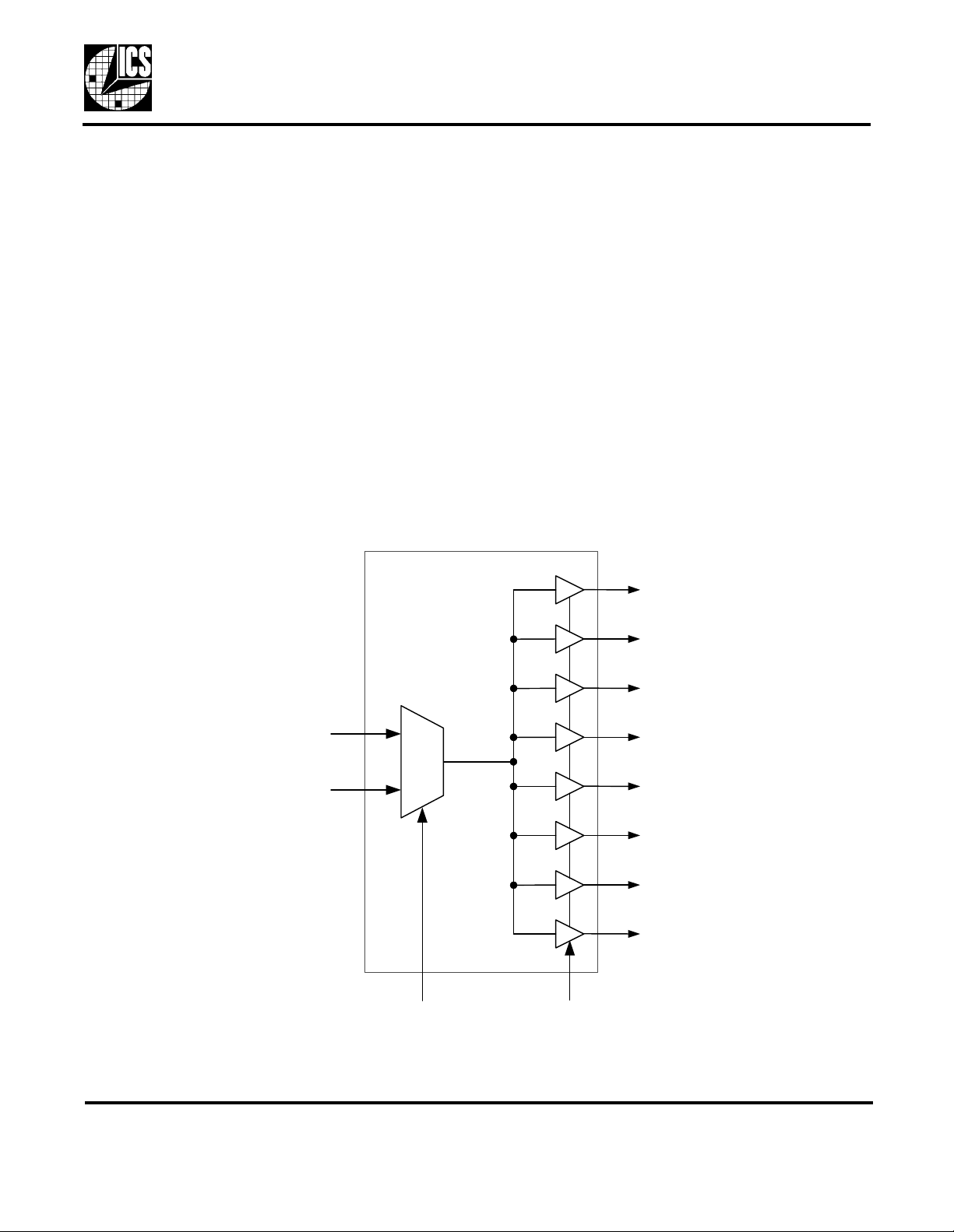
The ICS552-02 is a low skew, single-input to eight-
output clock buffer. It is part of ICS’ Clock Blocks
family. See the ICS553 for a 1 to 4 low skew buffer. For
more than 8 outputs see the MK74CBxxx Buffalo
series of clock drivers.
ICS makes many non-PLL and PLL based low skew
output devices as well as Z ero Delay Buffers to
synchronize clocks. Contact us for all of your clocking
needs.
TM
TM
Block Diagram
Features
• Extremely low skew outputs (50ps maximum)
• Packaged in 16 pin TSSOP
• Low power CMOS technology
• Operating Voltages of 2.5 V to 5 V
• Output Enable pin tri-states outputs
• 5 V tolerant input clocks
• Input/Output clock frequency up to 200 MHz
• Input clock multiplexer simplifies clock selection
Q0
IN A
IN B
1
0
SELA
Q1
Q2
Q3
Q4
Q5
Q6
Q7
OE
MDS 552-02 B 1 Revision 050401
Integrated Circuit Systems ● 525 Race Street, San Jose, CA 95 126 ● tel (408) 295-9800 ● www.icst.com

PRELIMINARY INFORMATION
LOW SKEW 2 INPUT MUX AND 1 TO 8 CLOCK
Pin Assignment Input Source Select
ICS552-02
OE
VDD
Q0
Q1
Q2
Q3
GND GND
INB
1
2
3
4
5
6
7
8
16 Pin TSSOP
Pin Descriptions
Pin
Number
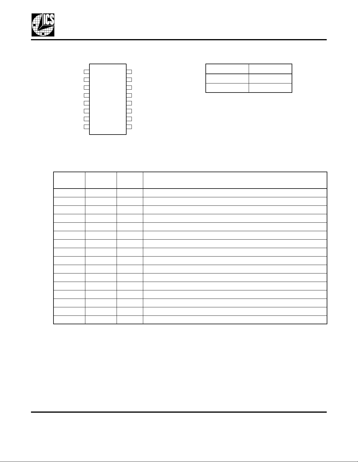
1 OE Input Output Enable. Tri-states outputs when low. Internal pull-up resistor.
2 VDD Power Connect to +2.5V, +3.3V or +5.0V. Must be the same as pin 15.
3 Q0 Output Clock Output 0
4 Q1 Output Clock Output 1
5 Q2 Output Clock Output 2
6 Q3 Output Clock Output 3
7 GND Power Connect to ground.
8 INB Input Clock Input B. 5V tolerant input.
9 INA Input Clock Input A. 5V tolerant input.
10 GND Power Connect to ground.
11 Q4 Output Clock Output 4
12 Q5 Output Clock Output 5
13 Q6 Output Clock Output 6
14 Q7 Output Clock Output 7
15 VDD Power Connect to + 2.5V, +3.3V or +5.0V. Must be the same as pin 2.
16 SELA Input Selects either INA or INB. Internal pull-up resistor.
Pin
Name
16
15
14
13
12
11
10
9
Type
Pin
SELA
VDD
Q7
Q6
Q5
Q4
INA
SELA Input
0INB
1INA
Pin Description
External Components
A minimum number of external components are required for proper operation. Decoupling capacitors of
0.01 µF should be connected between VDD on pin 2 and GND on pin 7, and between VDD on pin 15 and
GND on pin 10, as close to the device as possible. A 33 Ω series terminating resistor should be used on
each clock output if the trace is longer than 1 inch.
To achieve the low output skews that the ICS552-02 is capable of, careful attention must be paid to board
layout. Essentially, all 8 outputs must have identical terminations, identical loads, and identical trace
geometries. If they do not, the output skew will be degraded. For example, using a 30Ω series termination
on one output (with 33Ω on the others) will cause at least 15ps of skew.
MDS 552-02 B 2 Revision 050401
Integrated Circuit Systems ● 525 Race Street, San Jose, CA 95126 ● tel (408) 295-9800 ● www.icst.com
 Loading...