PRELIMINARY INFORMATION
ICS551
1 to 4 Clock Buffer
Description
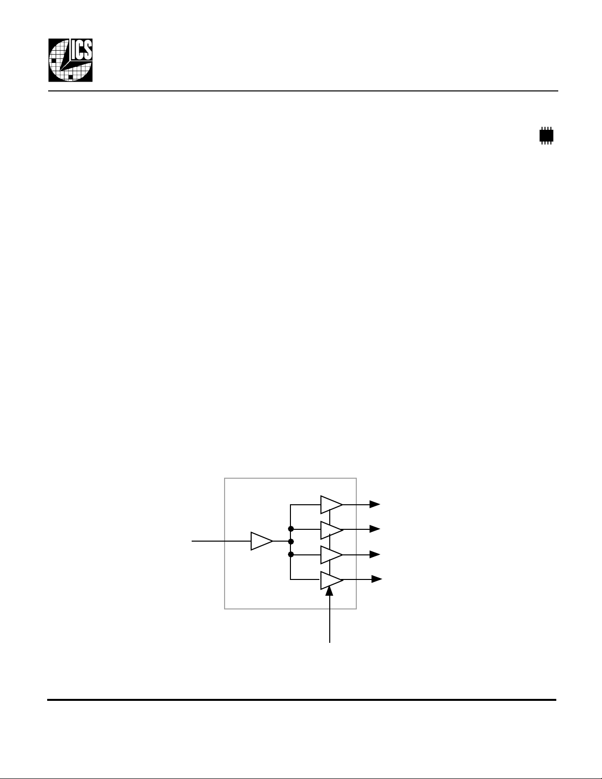
The ICS551 is a low cost, high speed single input
to four output clock buffer. Part of ICS’ Clock
BlocksTM family, this is our lowest cost, small clock
buffer. See the ICS552-01B for a monolithic dual
version of the ICS551 in a 20 pin QSOP.
ICS makes many non-PLL and PLL based low
skew output devices, as well as Zero Delay Buffers
to synchronize clocks. Contact us for all of your
clocking needs.
Features
• Packaged in 8 pin SOIC
• Low cost clock buffer
• Low skew (250ps) outputs
• Input/output clock frequency up to 160 MHz
• Operating voltages of 3.0 to 5.5 V
• Non-inverting
• Ideal for networking clocks
• Output Enable mode tri-states outputs
• Full CMOS clock swings with 25mA drive
capability at TTL levels
• Advanced, low power CMOS process
Block Diagram
Q1
Q2
ICLK
Q3
Q4
Output Enable
MDS 551 B 1 Revision 091200 Printed 11/14/00
Integrated Circuit Systems, Inc.•525 Race Street•San Jose•CA•95126•(408)295-9800tel•(408)295-9818fax

Pin Assignment
PRELIMINARY INFORMATION
ICS551
1 to 4 Clock Buffer
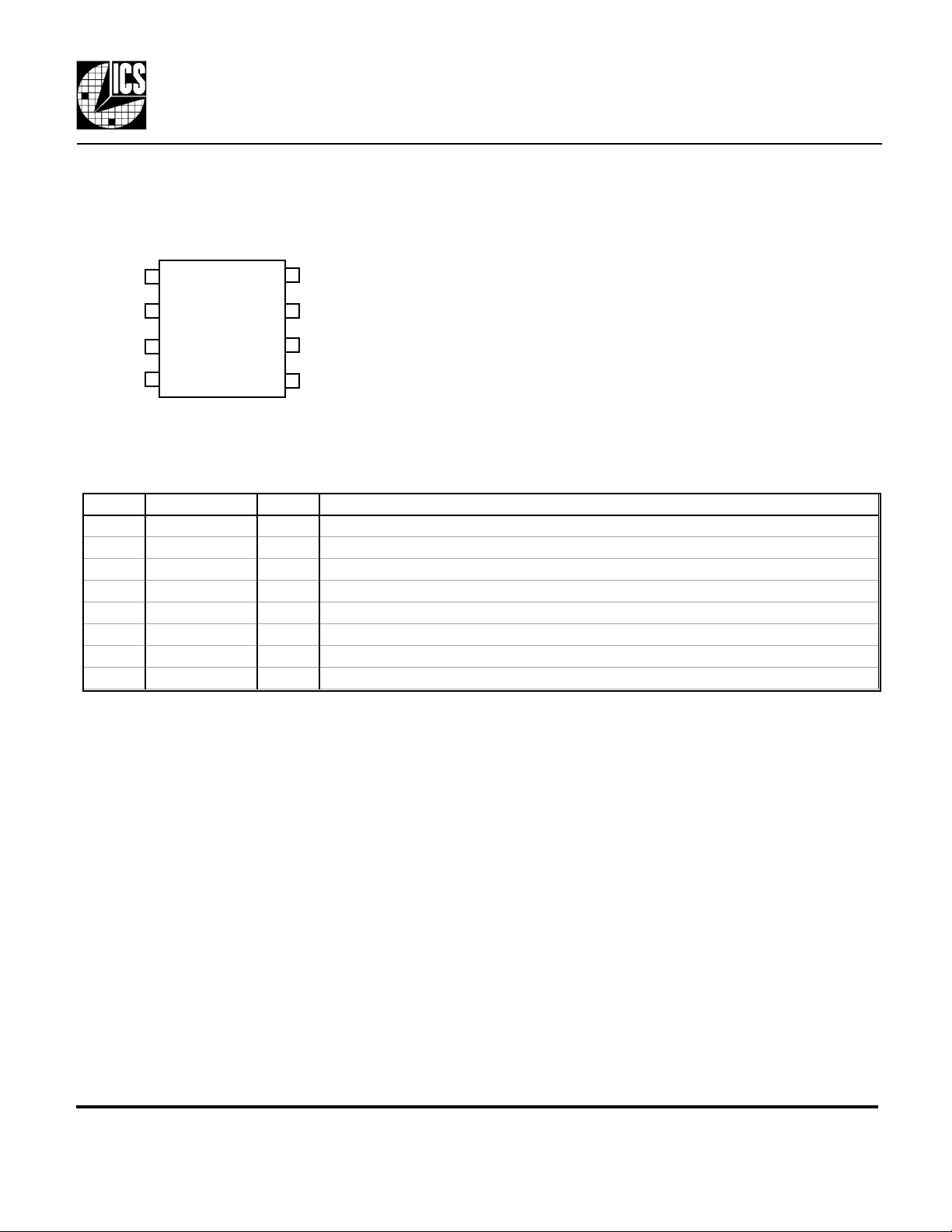
ICLK
Q1
Q2
Q3
1 8
2
3
4
OE
7
VDD
6
GND
5
Q4
8 pin SOIC
Pin Descriptions
Number Name Type Description
1 ICLK CI Clock input. Internal pull-up resistor.
2 Q1 O Clock Output 1.
3 Q2 O Clock Output 2.
4 Q3 O Clock Output 3.
5 Q4 O Clock Output 4.
6 GND P Connect to ground.
7 VDD P Connect to +3.3 V or +5.0 V.
8 OE I Output Enable. Tri-states outputs when low. Internal pull-up resistor.
Key: CI = clock input, I = input, O = output, P = power supply connection
External Components
A minimum number of external components are required for proper operation. A decoupling capacitor of
0.01 µF should be connected between VDD on pin 7 and GND on pin 6, and a 33 Ω terminating resistor
may be used on each clock output if the trace is longer than 1 inch.
MDS 551 B 2 Revision 091200 Printed 11/14/00
Integrated Circuit Systems, Inc.•525 Race Street•San Jose•CA•95126•(408)295-9800tel•(408)295-9818fax
 Loading...