ADVANCE INFORMATION
ICS548-03
Low Skew Clock Inverter and Divider
Description
The ICS548-03 is a low cost, low skew, high
performance general-purpose clock designed to
produce a set of one output clock, one inverted
output clock, and one clock divided-by-2. Using
our patented analog Phase-Locked Loop (PLL)
techniques, the device operates from a frequency
range from 10 MHz to 120 MHz in the PLL mode,
and up to 160 MHz in the non-PLL mode.
In applications that to need maintain low phase
noise in the clock tree, the non-PLL (when
S3=S2=1) mode should be used.
This chip is not a zero delay buffer. Many
applications may be able to use the ICS527 for zero
delay dividers.
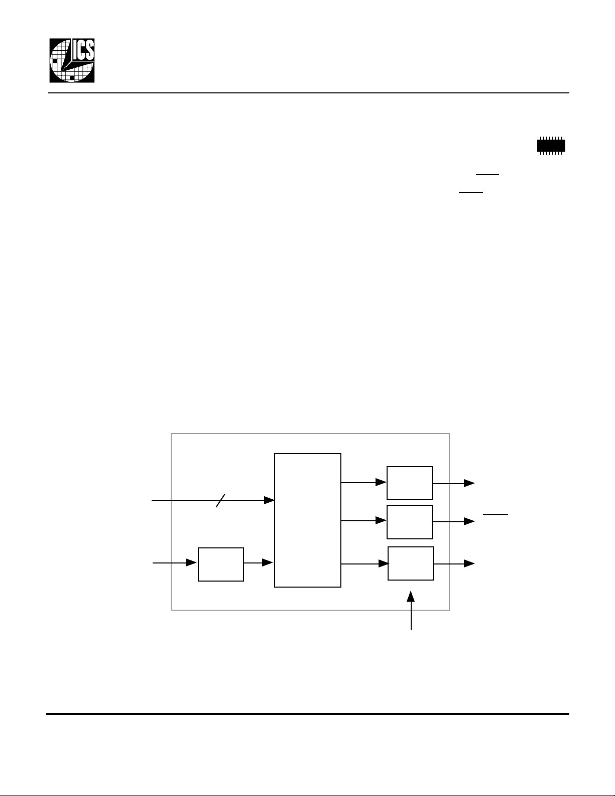
Block Diagram
Features
• Packaged in 16 pin narrow (150 mil) SOIC
• Input clock up to 160 MHz in the non-PLL mode
• Provides clock outputs of CLK, CLK, and CLK/2
• Low skew (500 ps) on CLK, CLK, and CLK/2
• All outputs can be tri-stated
• Entire chip can be powered down by changing one
or two select pins
• 3.3V or 5.0V operating voltage
Output
4
S3:S0
Clock Input
MDS 548-03 1 Revision 042700
Integrated Circuit Systems, Inc. • 525 Race Street • San Jose •CA•95126• (408) 295-9800tel • www.icst.com
Input
Buffer
Clock
Synthesis
and
Divider
Circuitry
Buffer
Output
Buffer
Output
Buffer
OE (All outputs)
CLK
CLK
CLK/2

ADVANCE INFORMATION
ICS548-03
Low Skew Clock Inverter and Divider
Pin Assignment
S3
S2
S0
1
2
3
4
5
6
7
8
ICLK DC
VDD
VDD
GND
GND
16
1415DC
13
12
11
10
9
DC
CLK
CLK
CLK/2
OE
S1
CLK, CLK, and CLK/2 Select Table (in MHz)
S3 S2 S1 S0 CLK, CLK CLK/2 PLL Input Range
0 0 0 0 Low Low Off Power down
0 0 0 1 Input/4 Input/8 On 20 -120
0 0 1 0 Input Input/2 On 20 -120
0 0 1 1 Input/2 Input/4 On 20 -120
0 1 0 0 Low Low Off Power down
0 1 0 1 Input x 2 Input On 20 - 60
0 1 1 0 Input/5 Input/10 On 20 -120
0 1 1 1 Input/3 Input/6 On 20 - 120
1 0 0 0 Low Low Off Power down
1 0 0 1 Input/4 Input/8 On 10 - 60
1 0 1 0 Input Input/2 On 10 - 60
1 0 1 1 Input/2 Input/4 On 10 - 60
1 1 0 0 Low Low Off Power down
1 1 0 1 Input/6 Input/12 Off 0 - 160
1 1 1 0 Input/8 Input/16 Off 0 - 160
1 1 1 1 Input/2 Input/4 Off 0 - 160
Pin Descriptions
Number Name Type Description
1 ICLK CI Input Clock. Connect to a CMOS level input clock.
2 VDD P Connect to +3.3V or +5.0V.
3 VDD P Connect to +3.3V or +5.0V.
4 S3 I Clock Select Pin 3. See above table.
5 GND P Connect to ground.
6 GND P Connect to ground.
7 S2 I Clock Select Pin 2. See above table.
8 S0 I Clock Select Pin 0. See above table.
9 S1 I Clock Select Pin 1. See above table.
10 OE I Output Enable. Tri-states all clock outputs when low.
11 CLK/2 O Clock Output divided by 2. See above table.
12 CLK O Clock Output. See above table.
13 CLK O Inverted Clock Output. See above table.
14 DC - Don't Connect. Do not connect anything to this pin.
15 DC - Don't Connect. Do not connect anything to this pin.
16 DC - Don't Connect. Do not connect anything to this pin.
Key: I = Input; O = Output; P = Power Supply connection; CI = Clock Input
MDS 548-03 2 Revision 042700
Integrated Circuit Systems, Inc. • 525 Race Street • San Jose •CA•95126• (408) 295-9800tel • www.icst.com
 Loading...