PRELIMINARY INFORMATION
ICS548-05A
MP3 Audio Clock
Description
The ICS548-05 is a low cost, low jitter, high
performance clock synthesizer designed to
produce audio sampling rates for MP3 systems.
Using ICS’ patented analog/digital Phase-Locked
Loop (PLL) techniques, the device uses an
inexpensive 3.6864 MHz crystal or clock input to
exactly produce all of the popular audio sampling
frequencies. Power down modes allow the chip to
be turned off completely, or the PLL and audio
clock output to be turned off separately.
ICS manufactures the largest variety of
multimedia clock synthesizers for all applications.
Consult ICS to eliminate VCXOs, crystals and
oscillators from your board.
Features
• Packaged in 16 pin TSSOP
• Ideal for Cirrus Logic’s MP3 chips
• Replaces multiple oscillators
• 3.3V (will work down to 2.7V) or 5V operation
• Uses an inexpensive 3.6864 MHz crystal or
clock input
• Supports 32 kHz, 44.1 kHz, 48 kHz, and 96 kHz
audio sampling rates
• Provides 128fs and 256fs clocks
• Zero ppm synthesis error
• Includes Power Down features
• Advanced, low power, sub-micron CMOS process
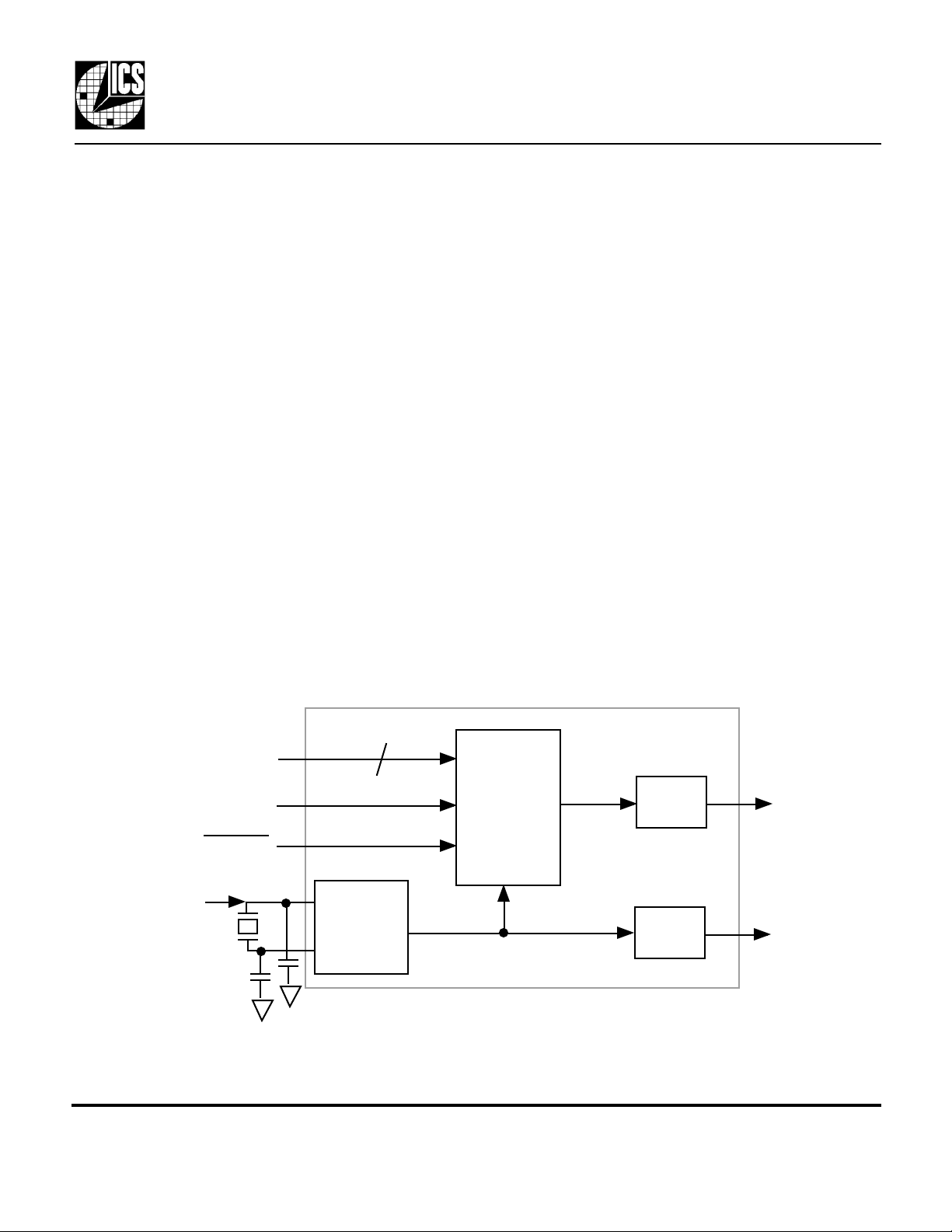
Block Diagram
3.6864 MHz
crystal or clock
S3:S0
REFEN
PDCLK
X1
Crystal
Oscillator
X2
Optional crystal capacitors
4
PLL/Clock
Synthesis
Circuitry
Output
Buffer
Output
Buffer
CLK
REFOUT
MDS 548-05 AC 1 Revision 032900
Integrated Circuit Systems, Inc. • 525 Race Street • San Jose •CA•95126•(408) 295-9800tel • www.icst.com

PRELIMINARY INFORMATION
Turns off PLL and stops CLK low
ICS548-05A
MP3 Audio Clock
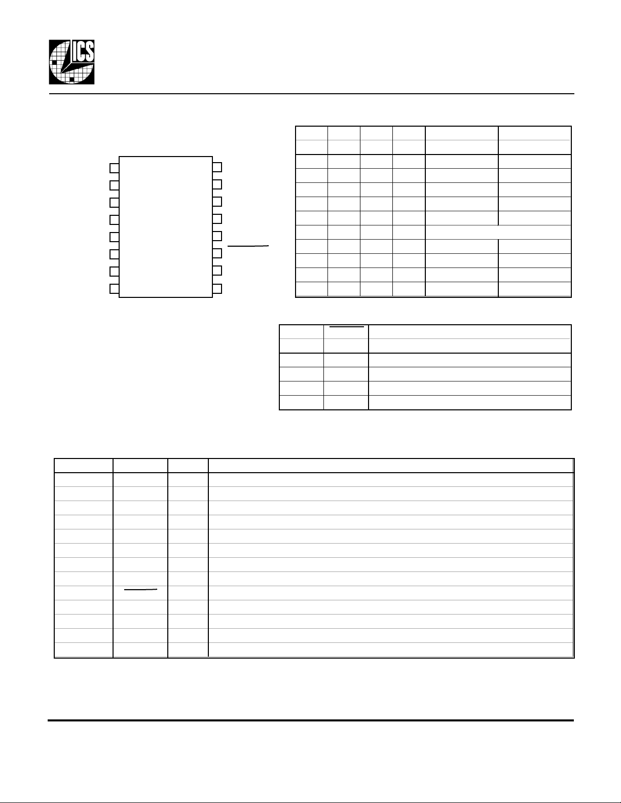
Pin Assignment
ICS548-05A
X1/ICLK
VDD
VDD
REFEN
GND
GND
S3
S2
Pin Descriptions
1
2
3
4
5
6
7
8
16 pin TSSOP
16
15
14
13
12
11
10
9
X2
DC
REFOUT
S0
S1
PDCLK
DC
CLK
Output Clock Select Table
S3 S2 S1 S0 Input (MHz) CLK (MHz)
Pin 7 Pin 8 Pin 12 Pin 13 Pins 1, (16) Pin 9
0 0 1 0 3.6864 2.8224
0 0 1 1 3.6864 3.072
1 0 0 0 3.6864 4.096
1 0 0 1 3.6864 5.6448
1 0 1 0 3.6864 6.144
1 0 1 1
1 1 0 0 3.6864 8.192
1 1 0 1 3.6864 11.2896
1 1 1 0 3.6864 12.288
1 1 1 1 3.6864 2.048
Power Down Clock Select Table
REFEN PDCLK Power Down Selection Mode
Pin 4 Pin 11
0 0 The entire chip is off.
0 1 PLL and CLK output run, REFOUT low.
1 0 REFOUT running, PLL off, CLK low.
1 1 All running.
Key: 0 = connect directly to GND
1 = connect directly to VDD
Number Name Type Description
1 X1/ICLK XI Crystal connection. Connect to a 3.6864 MHz crystal, or input clock.
2, 3 VDD P Connect to +3.3V or +5V. All VDDs must be same.
4 REFEN I Reference Clock Enable. See above table.
5, 6 GND P Connect to ground.
7 S3 I Frequency select pin 3. Determines clock outputs per table above.
8 S2 I Frequency select pin 2. Determines clock outputs per table above.
9 CLK O Audio clock output set by status of S0-S3. See table above.
10, 15 DC - Don't Connect. Do not connect anything to these pins.
11 PDCLK I Power Down Clock. See above table.
12 S1 I Frequency select pin 1. Determines clock outputs per table above.
13 S0 I Frequency select pin 0. Determines clock outputs per table above.
14 REFOUT O Buffered 3.6864 MHz oscillator output clock. Controlled by REFEN.
16 X2 XO Crystal connection. Connect to a 3.6864 MHz crystal, or leave unconnected for clock.
Key: I = Input; O = output; P = power supply connection; XI, XO = crystal connections
The input pins S3:S0 lack pull-ups, so they cannot be left floating. Tie directly to VDD or GND. For a
clock input, connect the input to X1, and leave X2 unconnected (floating).
MDS 548-05 AC 2 Revision 032900
Integrated Circuit Systems, Inc. • 525 Race Street • San Jose •CA•95126•(408) 295-9800tel • www.icst.com
 Loading...