

PRELIMINARY INFORMATION
ICS541
PLL Clock Divider
Description
The ICS541 is a cost effective way to produce a
high quality clock output divided from a clock
input. The chip accepts a clock input up to
135 MHz at 3.3 V, and by using proprietary Phase
Locked Loop (PLL) techniques, produces a divide
by 1, 2, 4, or 8 of the input clock. There are two
outputs on the chip, one being a low-skew divide
by two of the other. So, for instance, if an 80 MHz
input clock is used, the ICS541 can produce low
skew 80 MHz and 40 MHz clocks, or 40 MHz
and 20 MHz clocks, or 20 MHz and 10MHz
clocks. The chip has an all-chip power down mode
that stops the outputs low, and an OE pin that tristates the outputs.
The ICS541 is a member of the ICS
ClockBlocks™ family of clock building blocks.
See the ICS542 and ICS543 for other clock
dividers, and the ICS300, 501, 502, and 503 for
clock multipliers.
Features
• Packaged in 8 pin SOIC
• Low cost clock divider
• Low skew (500ps) outputs. One is ÷ 2 of other.
• Easy to use with other generators and buffers
• Input clock frequency up to 135 MHz at 3.3 V
• Input clock frequency up to 156 MHz at 5.0 V
• Tolerant of poor input clock duty cycle, jitter.
• Output clock duty cycle of 45/55
• Power Down turns off chip
• Output Enable
• Full CMOS clock swings with 25mA drive
capability at TTL levels
• Advanced, low power CMOS process
• Operating voltages of 3.0 to 5.5 V
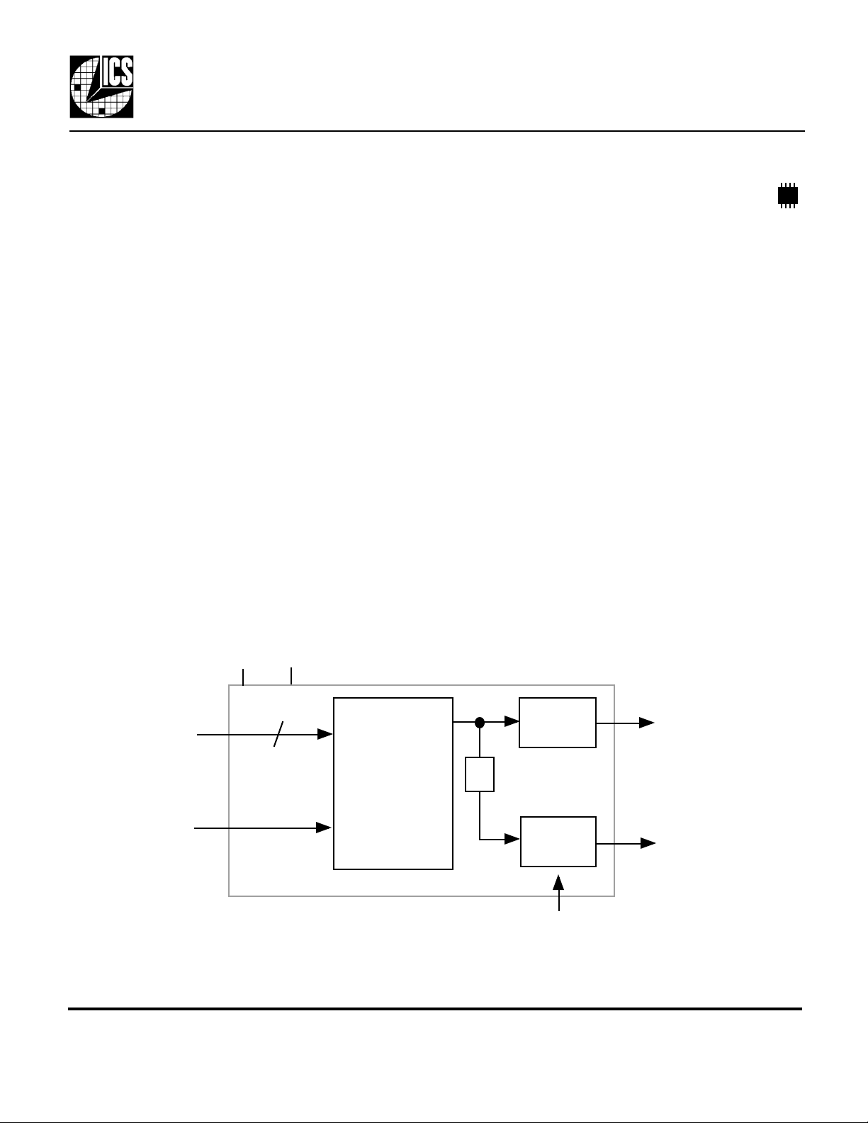
Block Diagram
S1, S0
Input Clock
VDD GND
2
PLL,
Divider and
Selection
Circuitry
Output
Buffer
÷2
Output
Buffer
OE (both outputs)
CLK
CLK/2
MDS 541 B 1 Revision 082500 Printed 11/14/00
Integrated Circuit Systems, Inc. •525 Race Street• San Jose•CA• 95126• (408)295-9800tel • www.icst.com

PRELIMINARY INFORMATION
Power Down All
ICS541
PLL Clock Divider
Pin Assignment
ICLK
VDD
GND
S0
1 8
2
3
4
7
6
5
CLK
CLK/2
OE
S1
Clock Decoding Table
S1 S0 CLK CLK/2
#5 #4 pin #8 pin #7
0 0
0 1 Input/4 Input/8
1 0 Input Input/2
1 1 Input/2 Input/4
0 = connect directly to ground.
8 pin SOIC
1 = connect directly to VDD.
Pin Descriptions
Number Name Type Description
1 ICLK CI Clock input.
2 VDD P Connect to +3.3V or +5V.
3 GND P Connect to ground.
4 S0 I Select 0 for output clock. Connect to GND or VDD, per decoding table above.
5 S1 I Select 1 for output clock. Connect to GND or VDD, per decoding table above.
6 OE I Output Enable. Tri-states both output clocks when low.
7 CLK/2 O Clock output per Table above. Low skew divide by two of pin 8 clock.
8 CLK O Clock output per Table above.
Key: CI = clock input, I = input, O = output, P = power supply connection
External Components
The ICS541 requires a 0.01 µF decoupling capacitor to be connected between VDD and GND. It must
be connected close to the ICS541 to minimize lead inductance. No external power supply filtering is
required for this device. A 33 Ω terminating resistor can be used next to each output pin. If a 3.3 V input
clock is applied to the ICLK pin, with the ICS541 at 5 V, the clock must be AC coupled.
MDS 541 B 2 Revision 082500 Printed 11/14/00
Integrated Circuit Systems, Inc. •525 Race Street• San Jose•CA• 95126• (408)295-9800tel • www.icst.com
 Loading...