User Configurable Zero Delay Buffer
Description Features
The ICS527-01 Clock Slicer™ is the most flexible
way to generate an output clock from an input
clock with zero skew. The user can easily configure
the device to produce nearly any output clock that
is multiplied or divided from the input clock. The
part supports non-integer multiplications and
divisions. A SYNC pulse indicates the rising clock
edges that are aligned with zero skew. Using
Phase-Locked Loop (PLL) techniques, the device
accepts an input clock up to 200 MHz and
produces an output clock up to 160 MHz.
The ICS527-01 aligns rising edges on ICLK and
FBIN at a ratio determined by the reference and
feedback dividers.
For configurable clocks that do not require
zero delay, use the ICS525.
• Packaged as 28 pin SSOP (150 mil body)
• Synchronizes fractional clocks rising edges
• User determines the output frequency - no
software needed
• Slices frequency or period
• SYNC pulse output indicates aligned edges
• Input clock frequency of 600 kHz - 200 MHz
• Output clock frequencies up to 160 MHz
• Very low jitter
• Duty cycle of 45/55 up to 160 MHz
• Operating voltage of 3.3 V (±10%)
• Pin selectable double drive strength
• Multiple outputs available when combined with
Buffalo clock drivers
ICS527-01
Clock Slicer™
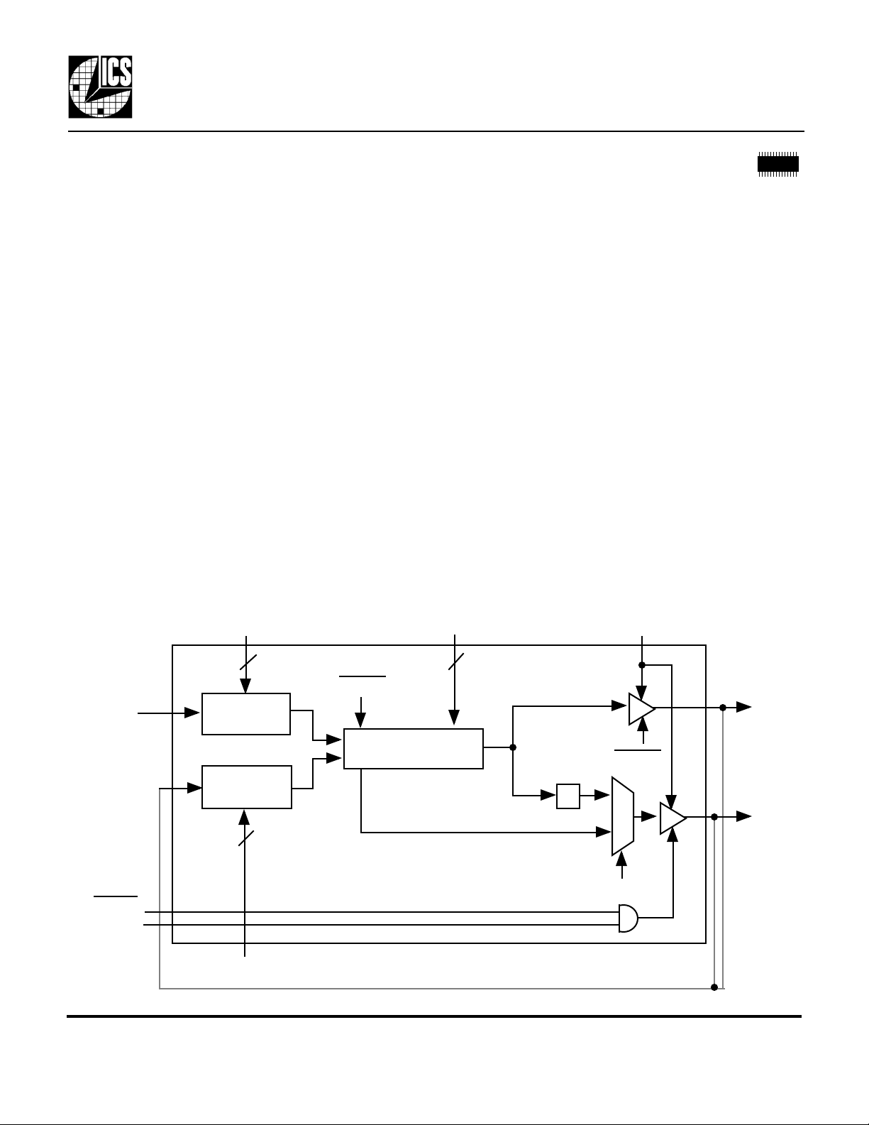
Block Diagram
ICLK
FBIN
PDTS
OECLK2
R6:R0
7
Reference
Divide
Feedback
Divide
7
PDTS
PLL
• Zero input to output skew
• Industrial temperature version available
• Advanced, low power CMOS process
S1:S0
2
÷2
SYNC
2XDRIVE
PDTS
1
0
DIV2
CLK1
CLK2
F6:F0
MDS 527-01 B 1 Revision 020801
Integrated Circuit Systems, Inc. • 525 Race Street • San Jose • CA•95126•(408)295-9800tel • www.icst.com
External feedback from CLK1 or CLK2 (not both).

ICS527-01
CLK1 Output Frequency (MHz)
Clock Slicer™
User Configurable Zero Delay Buffer
Pin Assignment
R5
1
2
R6
S0
S1
F0
F1
F2
3
4
5
6
7
8
9
10
11
12
13
14
DIV2
VDD
ICLK
FBIN
GND
OECLK2
2XDRIVE
Pin Description
28
27
26
25
24
23
22
21
20
19
18
17
16
15
R4
R3
R2
R1
R0
VDD
CLK1
CLK2
GND
PDTS
F6
F5
F4
F3
Frequency Configuration Table
S1 S0
pin 5 pin 4 0 to 70° -40 to 85°
0 0 37 - 75 35 - 70
0 1 18 - 37 16 - 35
1 0 4 - 10 4 - 8
1 1 75 - 160 70 - 140
To cover the range from 10-18 MHz (0-70 °C) and 8-16
(-40-85°C), select address 01 to generate 2x your desired output
frequency, then configure CLK2 to generate CLK1/2
CLK2 Operation Table
OECLK2 DIV2 CLK2
0 X Z
1 0 SYNC
1 1 CLK1/2
Clock Drive Select Table
2XDRIVE OUTPUT DRIVE
0 12 mA
1 25 mA
Pin # Name Type Description
1, 2, 24-28 R5, R6, R0-R4 I(PU) Reference divider word input pins determined by user. Forms a binary number from 0 to 127.
3 DIV2 I(PU) Selects CLK2 function to output a SYNC signal or a divide by 2 of CLK1. See table above.
4, 5 S0, S1 I(PU) Select pins for output divider determined by user. See table above.
6, 23 VDD P Connect to VDD.
7 ICLK I Reference clock input.
8 FBIN I Feedback clock input.
9, 20 GND P Connect to ground.
10 OECLK2 I(PU) CLK2 Output Enable. CLK2 tri-stated when low.
11 2XDRIVE I(PU) Clock output drive strength doubled when high.
12-18 F0-F6 I(PU) Feedback divider word input pins determined by user. Forms a binary number from 0 to 127.
19 PDTS I(PU) Power Down. Active low. Turns off entire chip when low. Both Clock outputs tri-stated.
21 CLK2 O Output Clock 2. Can be the SYNC output or a low skew divide by 2 of CLK1.
22 CLK1 O Output Clock 1.
Key: I = Input; I(PU) = Input with internal pull-up resistor; I = Input; O = Output; P = Power supply
connection
MDS 527-01 B 2 Revision 020801
Integrated Circuit Systems, Inc. • 525 Race Street • San Jose • CA•95126•(408)295-9800tel • www.icst.com

ICS527-01
Clock Slicer™
User Configurable Zero Delay Buffer
Using the Clock Slicer™
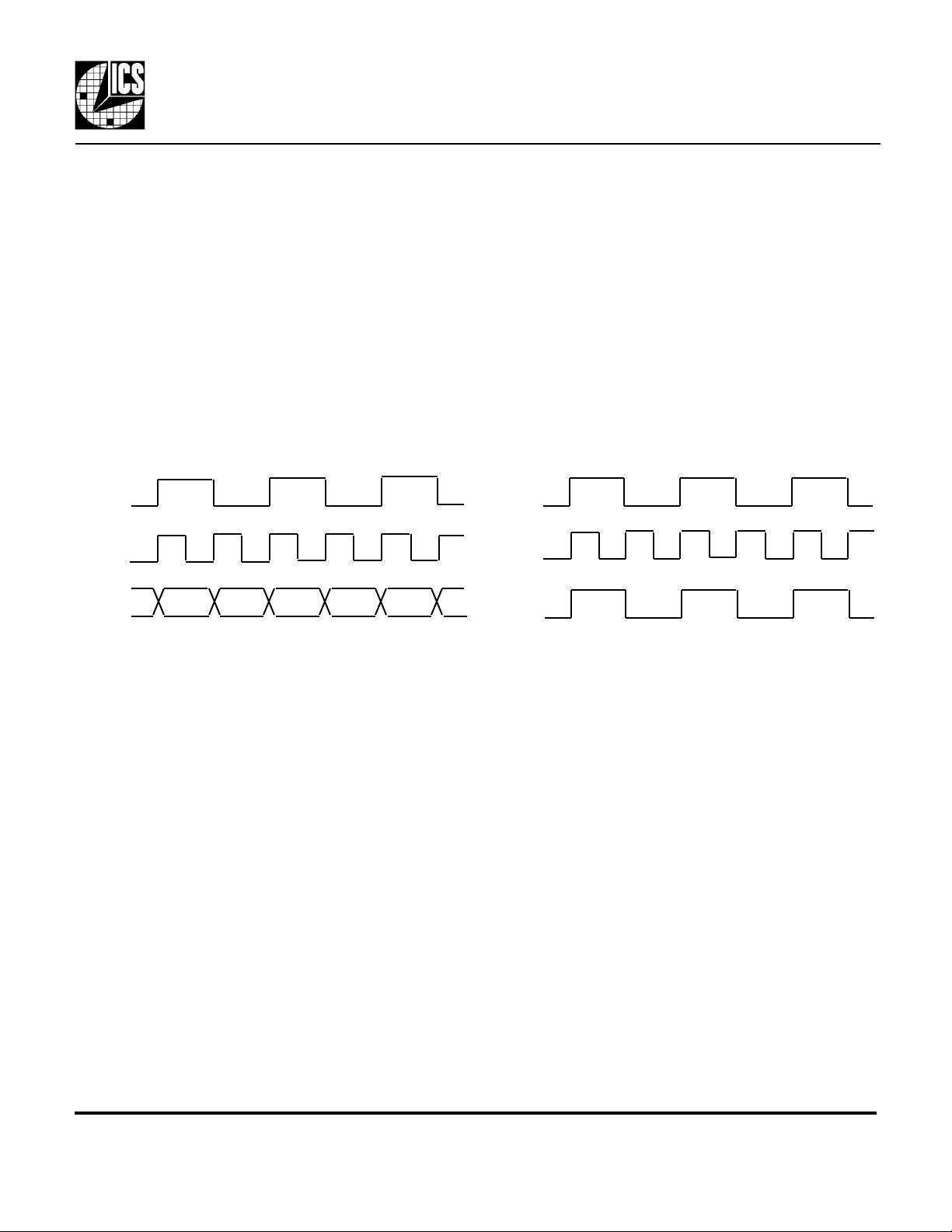
First use DIV2 to select the function of the CLK2 output. If DIV2 is high, a divide-by-2, low skew version
of CLK1 is present on CLK2. If DIV2 is low, a SYNC pulse is generated on CLK2. The SYNC pulse goes
high synchronously with the rising edges of ICLK and CLK1 that are de-skewed. The SYNC function
operates at CLK1 frequencies up to 66 MHz. If neither CLK1/2 or a SYNC pulse are required, then CLK2
should be disabled by connecting OECLK2 to ground, which will also give the lowest jitter on CLK1.
Next, the feedback scheme should be chosen. If CLK2 is being used as a SYNC or is tri-stated, then CLK1
must be connected to FBIN. If CLK2 is selected to be CLK1 divided-by-2 (DIV2 = 1, OECLK2 = 1),
then either CLK1 or CLK2 must be connected to FBIN. The choice between CLK1 or CLK2 is illustrated
by the following example where the device has been configured to generate CLK1 that is twice the
frequency on ICLK.
ICLK
CLK1
CLK2
CLK1 Feedback
Using CLK1 as the feedback will always result in synchronized rising edges between ICLK and CLK1. But
CLK2 could be a falling edge compared with ICLK. Therefore, wherever possible, we recommend the use
of CLK2 feedback. This will synchronize the rising edges of all 3 clocks.
More complicated feedback schemes can be used, such as incorporating multiple output buffers in the
feedback path. An example of this is given later in the datasheet. The fundamental property of the
ICS527-01 is that it aligns rising edges on ICLK and FBIN at a ratio determined by the reference and
feedback dividers.
The drive strength is selected by the 2XDRIVE pin. If high drive strength is not required, we recommend
tying this pin low.
Lastly, the divider settings should be selected. The following section describes how the dividers can be set.
ICLK
CLK1
CLK2
CLK2 Feedback
MDS 527-01 B 3 Revision 020801
Integrated Circuit Systems, Inc. • 525 Race Street • San Jose • CA•95126•(408)295-9800tel • www.icst.com
 Loading...