

Datasheet ICS525-01R, ICS525-01RI, ICS525-01RIT, ICS525-01RT, ICS525R-02I Datasheet (ICST)
...
OSCaR™ User Configurable Clock
p
Description Features
The ICS525-01 and ICS525-02 OSCaR™ are
the most flexible way to generate a high quality,
high accuracy, high frequency clock output from
an inexpensive crystal or clock input. The name
OSCaR stands for OSCillator Replacement, as
they are designed to replace crystal oscillators in
almost any electronic system. The user can easily
configure the device to produce nearly any
output frequency from any input frequency by
grounding or floating the select pins. Neither
microcontroller nor software nor device
programmer are needed to set the frequency.
Using Phase-Locked-Loop (PLL) techniques, the
device accepts a standard fundamental mode,
inexpensive crystal to produce output clocks up
to 250 MHz. It can also produce a highly
accurate output clock from a given input clock,
keeping them frequency locked together.
For similar capability with a serial interface, use
the ICS307. For simple multipliers to produce
common frequencies, refer to the LOCO family
of parts, which are smaller and more cost
effective.
• Packaged as 28 pin SSOP (150 mil body)
• ICS525-01 with output frequencies up to 160 MHz
• ICS525-02 with output frequencies up to 250 MHz
• User determines the output frequency by
setting all internal dividers
• Eliminates need for custom oscillators
• No software needed
• Online ICS525 calculator at
www.icst.com/products/ics525inputForm.html
• Pull-ups on all select inputs
• Input crystal frequency of 5 - 27 MHz
• Input clock frequency of 2 - 50 MHz
• Very low jitter
• Duty cycle of 45/55 up to 200 MHz
• Operating voltages of 3.0 to 5.5V
• Ideal for oscillator replacement
• Industrial temperature versions available
• For Zero Delay, refer to the ICS527
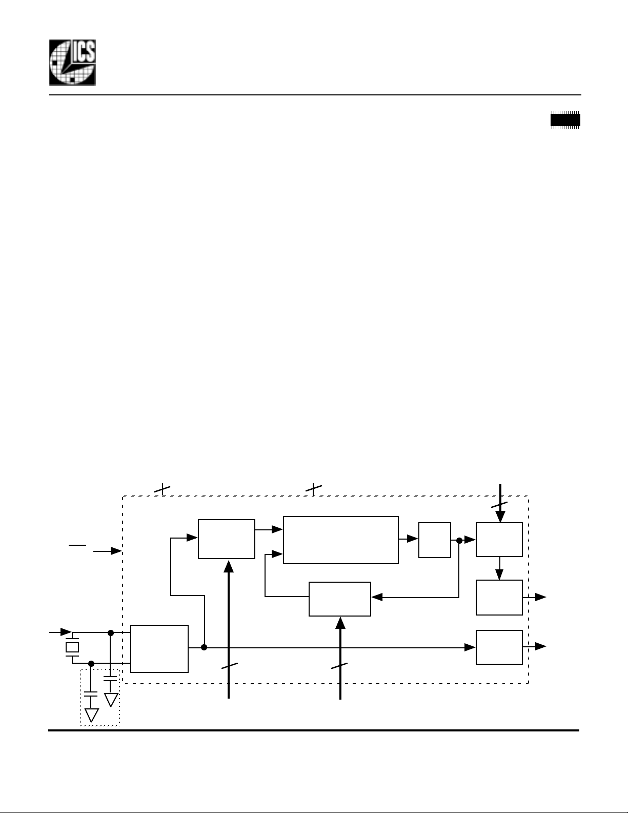
ICS525-01/02
Block Diagram
VDD GND S2:S0
2
Reference
PD
Crystal or
clock in
MDS 525-01/02 I 1Revision 071100 Printed 11/13/00
Integrated Circuit Systems, Inc. • 525 Race Street •San Jose• CA • 95126•(408) 295-9800tel• www.icst.com
ut
X1/ICLK
Crystal
Oscillator
X2
optional
Divider
7
R6:R0 V8:V0
Phase Comparator,
2
Charge Pump,
and Loop Filter
VCO
Divider
9
VCO
3
Output
Divider
Output
Buffer
Output
Buffer
CLK
REF
ICS525-01/02
OSCaR™ User Configurable Clock
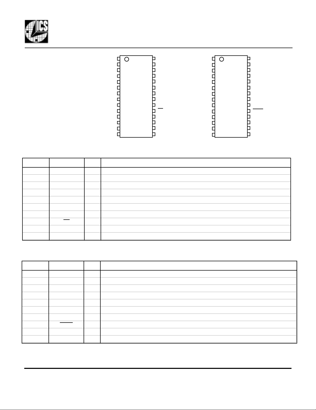
Pin Assignments
R5
R6
S0
S1
S2
VDD
X1/ICLK
X2
GND
V0
V1
V2
V3
V4
1
2
3
4
5
6
7
8
9
10
11
12
13
14
28
27
26
25
24
23
22
21
20
19
18
17
16
15
R4
R3
R2
R1
R0
VDD
REF
CLK
GND
PD
V8
V7
V6
V5
R5
R6
S0
S1
S2
VDD
X1/ICLK
X2
GND
V0
V1
V2
V3
V4
1
2
3
4
5
6
7
8
9
10
11
12
13
14
28
27
26
25
24
23
22
21
20
19
18
17
16
15
R4
R3
R2
R1
R0
VDD
REF
CLK
GND
PDTS
V8
V7
V6
V5
ICS525-01 ICS525-02
ICS525-01 Pin Descriptions
Pin # Name Type Description
1, 2, 24-28 R5, R6, R0-R4 I(PU) Reference divider word input pins determined by user. Forms a binary number from 0 to 127.
3, 4, 5 S0, S1, S2 I(PU) Select pins for output divider determined by user. See table on page 3.
6, 2 3 VDD P Connect to VDD.
7 X1/ICLK X1 Crystal connection. Connect to a parallel resonant fundamental crystal, or input clock.
8 X2 X2 Crystal connection. Connect to a crystal, or leave unconnected for clock.
9, 20 GND P Connect to ground.
10-18 V0-V8 I(PU) VCO divider word input pins determined by user. Forms a binary number from 0 to 511.
19 PD I(PU) Power Down. Active low. Turns off entire chip when low. Clock outputs stop low.
21 CLK O Output Clock determined by status of R0-R6, V0-V8, S0-S2 and input frequency.
22 REF O Reference output. Buffered crystal oscillator (or clock) output.
ICS525-02 Pin Descriptions
Pin # Name Type Description
1, 2, 24-28 R5, R6, R0-R4 I(PU) Reference divider word input pins determined by user. Forms a binary number from 0 to 127.
3, 4, 5 S0, S1, S2 I(PU) Select pins for output divider determined by user. See table on page 3.
6, 2 3 VDD P Connect to VDD.
7 X1/ICLK X1 Crystal connection. Connect to a parallel resonant fundamental crystal, or input clock.
8 X2 X2 Crystal connection. Connect to a crystal, or leave unconnected for clock.
9, 20 GND P Connect to ground.
10-18 V0-V8 I(PU) VCO divider word input pins determined by user. Forms a binary number from 0 to 511.
19 PDTS I(PU) Power Down and Tri-state. Active low. Turns off entire chip and tri-states the outputs when low.
21 CLK O Output Clock determined by status of R0-R6, V0-V8, S0-S2 and input frequency.
22 REF O Reference output. Buffered crystal oscillator (or clock) output.
Key: I(PU) = Input with internal pull-up resistor; X1, X2 = Crystal connections; O = Output;
P = Power supply connection
MDS 525-01/02 I 2Revision 071100 Printed 11/13/00
Integrated Circuit Systems, Inc. • 525 Race Street •San Jose• CA • 95126•(408) 295-9800tel• www.icst.com
OSCaR™ User Configurable Clock
q
p
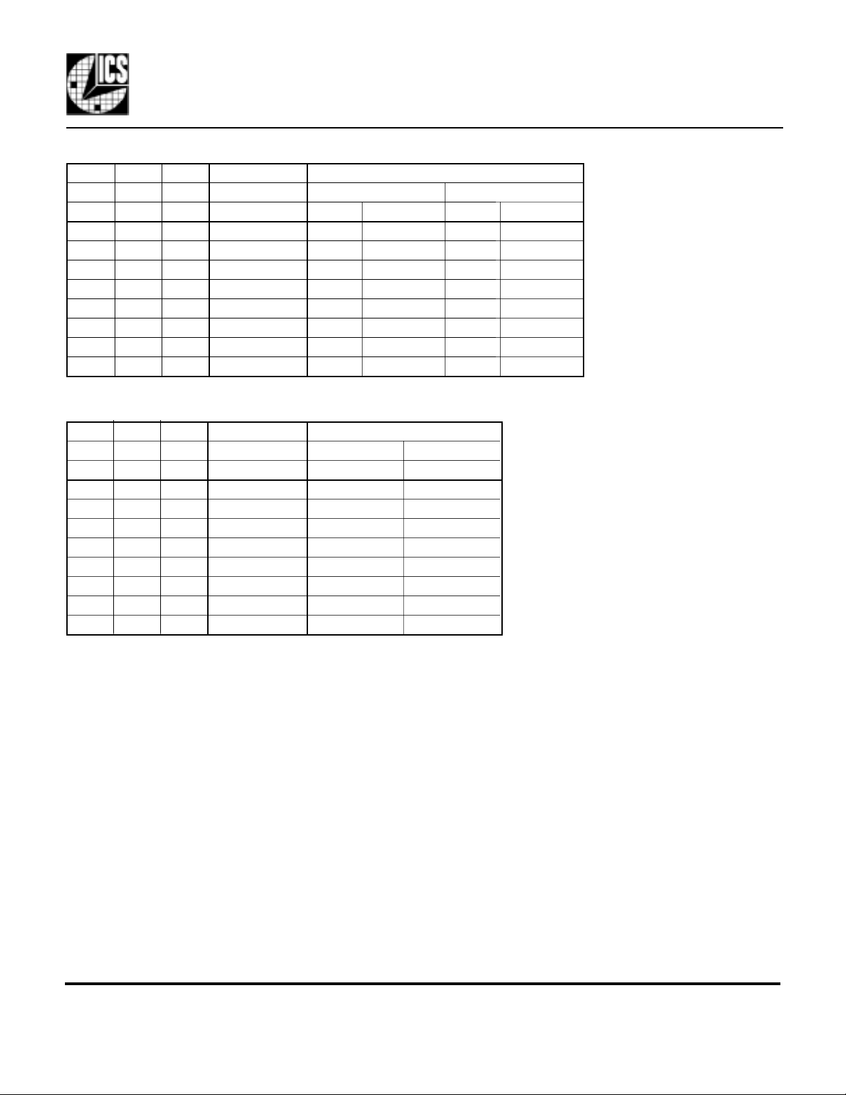
ICS525-01 Output Divider and Maximum Output Frequency Table
ICS525-01/02
S2 S1 S0 CL K
pin 5 pin 4 pin 3 Output Divider VDD = 5 V VDD = 3.3V
000 10 26 23 18 16
001 2 160 140 100 90
010 8 40 36 25 22
011 4 80 72 50 45
100 5 50 45 34 30
101 7 40 36 26 23
110 9 33.3 30 20 18
111 6 53 47 27 24
Max. Output Frequency ((MHz)
0-70 °C -40 to +85 °C 0-70 °C -40 to +85 °C
ICS525-02 Output Divider and Maximum Output Frequency Table
S2 S1 S0 CLK
pin 5 pin 4 pin 3 Output Divider VDD = 5V VDD = 3.3V
0 0 0 6 67 40
0 0 1 2 200 120
0 1 0 8 50 30
0 1 1 4 100 60
1 0 0 5 80 48
1 0 1 7 57 34
1 1 0 1 250 200
1 1 1 3 133 80
Max. Output Frequency (MHz)
-40 to +85 °C -40 to +85 °C
The ICS525-02 is only offered in the
industrial tem
erature range.
External Components / Crystal Selection
The ICS525 requires two 0.01µF decoupling capacitors to be connected between VDD and GND, one on
each side of the chip. They must be connected close to the ICS525 to minimize lead inductance. No
external power supply filtering is required for this device. A 33Ω series terminating resistor can be used
next to the CLK and REF pins. The approximate total on-chip capacitance for a crystal is 16pF, so a
parallel resonant, fundamental mode crystal with this value of load (correlation) capacitance should be
used. For example, using the ICS525-01 with crystals having a specified load capacitance greater than
16 pF, crystal capacitors may be connected from each of the pins X1 and X2 to Ground as shown in the
Block Diagram on page 1. The value (in pF) of these crystal caps should be = (CL-16)*2, where CL is the
crystal load capacitance in pF. These external capacitors are only required for applications where the exact
fre
uency is critical. For a clock input, connect to X1 and leave X2 unconnected (no capacitors on either).
MDS 525-01/02 I 3Revision 071100 Printed 11/13/00
Integrated Circuit Systems, Inc. • 525 Race Street •San Jose• CA • 95126•(408) 295-9800tel• www.icst.com

ICS525-01/02
g op
p
p
p
p
q
p
p
p
OSCaR™ User Configurable Clock
Determining (setting) the output frequency
The user has full control in setting the desired output frequency over the range shown in the table on
page 2. To replace a standard oscillator, a user should connect the divider select input pins directly to
ground (or VDD, although this is not required because of internal pull-ups) during Printed Circuit Board
layout, so that the ICS525 automatically produces the correct clock when all components are soldered. It is
also possible to connect the inputs to parallel I/O ports to switch frequencies. By choosing divides
carefully, the number of inputs which need to be changed can be minimized. Observe the restrictions
stated below on allowed values of VDW and RDW.
ICS525-01 Settings
Use the online ICS525 calculator at www.icst.com/products/ics525inputForm.html or alternatively, the
out
ut of the ICS525-01 can be determined by the following simple equation:
CLK frequency = Input frequency • 2 •
Where Reference Divider Word (RDW) = 1 to 127 (0 is not permitted)
VCO Divider Word (VDW) = 4 to 511 (0, 1, 2, 3 are not permitted)
Out
ut Divider (OD) = values on page 3
Also, the followin
10 MHz < In
200 kHz <
ICS525-02 Settings
Use the online ICS525 calculator at www.icst.com/products/ics525inputForm.html or alternatively, the
out
ut of the ICS525-02 can be determined by the following simple equation:
CLK fre
Where Reference Divider Word (RDW) = 0 to 127
erating ranges should be observed:
ut frequency • 2 •
Input Frequency
(RDW+2)
uency = Input frequency • 2 •
VCO Divider Word (VDW) = 0 to 511
Out
ut Divider (OD) = values on page 3
(VDW+8)
(RDW+2)
(VDW+8)
(RDW+2)(OD)
< 320 MHz at 5.0V or
< 200 MHz at 3.3V
(VDW+8)
(RDW+2)(OD)
See Table on Page 3
for full details of
[ ]
maximum out
ut.
Also, the following operating ranges should be observed:
10 MHz < In
200 kHz <
MDS 525-01/02 I 4Revision 071100 Printed 11/13/00
Integrated Circuit Systems, Inc. • 525 Race Street •San Jose• CA • 95126•(408) 295-9800tel• www.icst.com
ut frequency • 2 •
Input Frequency
(RDW+2)
(VDW+8)
(RDW+2)
< 400 MHz at 5.0V or
< 240 MHz at 3.3V
See Table on Page 3
for full details of
[ ]
maximum output.

ICS525-01/02
q
OSCaR™ User Configurable Clock
The dividers are expressed as integers, so that if a 66.66 MHz output is desired from a 14.31818 input, the
Reference Divider Word (RDW) should be 59, and the VCO Divider Word (VDW) should be 276, with
an Output divider (OD) of 2. In this example, R6:R0 is 0111011, V8:V0 is 100010100, and S2:S0 is 001.
Since all of these inputs have pull-up resistors, it is only necessary to ground the zero pins, namely V7, V6,
V5, V3, V1, V0, R6, R2, S2, and S1.
To determine the best combination of VCO, reference, and output divider, use the ICS525 Calculator on
our Web site: http://www.icst.com/products/ics525inputForm.html. This online form is easy to use and
quickly shows you up to three options for these settings.
You may also fax this page to MicroClock/ICS at 408 295 9818(fax), or contact us via our website at
www.icst.com. Be sure to indicate the following:
Your Name ________________ Company Name___________________ Telephone_________________
Respond by e-mail (list your e-mail address) __________________or fax number ___________________
Desired input crystal/clock (in MHz) _______________ Desired output frequency________________
VDD = 3.3V or 5V ___________ Duty Cycle: 40-60% _______ or 45-55% re
uired________
MDS 525-01/02 I 5Revision 071100 Printed 11/13/00
Integrated Circuit Systems, Inc. • 525 Race Street •San Jose• CA • 95126•(408) 295-9800tel• www.icst.com

ICS525-01/02
OSCaR™ User Configurable Clock
Electrical Specifications
Parameter Conditions Minimum Typical Maximum Units
ABSOLUTE MAXIMUM RATINGS (stresses beond these can permanentl damage the device)
Supply Voltage, VDD Referenced to GND 7 V
Inputs Referenced to GND -0.5 VDD+0.5 V
Clock Output Referenced to GND -0.5 VDD+0.5 V
Ambient Operating Temperature Commercial 0 70 °C
Industrial -40 85 °C
Soldering Temperature Max of 10 seconds 260 °C
Storage Temperature -65 150 °C
DC CHARACTERISTICS (VDD = 3.3 V unless otherwise noted)
Operating Voltage, VDD 3 5.5 V
Input High Voltage, VIH 2 V
Input Low Voltage, VIL 0.8 V
Input High Voltage, VIH, X1/ICLK only ICLK (Pin 7) (VDD/2)+1 VDD/2 V
Input Low Voltage, VIL, X1/ICLK only ICLK (Pin 7) VDD/2 (VDD/2)-1 V
Output High Voltage, VOH IOH = -12 mA VDD-0.4 V
Output Low Voltage, VOL IOL=12 mA 0.4 V
IDD Operating Supply Current, 15 MHz crystal 60MHz out, No Load 8 mA
IDD Operating Supply Current, Power Down Pin 19=0 7 µA
Short Circuit Current CLK and REF outputs ±55 mA
On-Chip Pull-up Resistor All V, R, S pins and pin 19 270 kΩ
Input Capacitance All V, R, S pins and pin 19 4 pF
MDS 525-01/02 I 6Revision 071100 Printed 11/13/00
Integrated Circuit Systems, Inc. • 525 Race Street •San Jose• CA • 95126•(408) 295-9800tel• www.icst.com

ICS525-01/02
p
OSCaR™ User Configurable Clock
Electrical Specifications (cont.)
Parameter Conditions Minimum Typical Maximum Units
AC CHARACTERISTICS (VDD = 3.3 V unless otherwise noted)
Input Frequency, crystal input 5 27 MHz
Input Frequency, clock input 0.5 50 MHz
Output Frequency, VDD = 4.5 to 5.5V 0 °C to 70 °C 1 160
ICS525-01, note 1 -40 °C to +85 °C 1 140 MHz
Output Frequency, VDD = 3.0 to 3.6V 0 °C to 70 °C 1 100
ICS525-01, note 1 -40 °C to +85 °C 1 90 MHz
Output Frequency, VDD = 4.5 to 5.5V
ICS525-02, note 1 -40 °C to +85 °C 1.5 250 MHz
Output Frequency, VDD = 3.0 to 3.6V
ICS525-02, note 1 -40 °C to +85 °C 1 200 MHz
Output Clock Rise Time 0.8 to 2.0V 1 ns
Output Clock Fall Time 2.0 to 0.8V 1 ns
Output Clock Duty Cycle, OD = 2, 4, 6, 8, or 10 at VDD/2 45 49 to 51 55 %
Output Clock Duty Cycle, OD = 3, 5, 7, or 9 at VDD/2 40 60 %
Output Clock Duty Cycle, OD = 1 (-02 only) at VDD/2 35 65
Power Down Time, PD low to clocks stopped 50 ns
Power Up Time, PD high to clocks stable 10 ms
Absolute Clock Period Jitter, ICS525-01, Note 2 Deviation from mean ±140 ps
One Sigma Clock Period Jitter, ICS525-01, Note 2 One Sigma 45 ps
Absolute Clock Period Jitter, ICS525-02, Note 2 Deviation from mean ±85 ps
One Sigma Clock Period Jitter, ICS525-02, Note 2 One Sigma 30 ps
Note 1: The phase relationship between input and output can change at power up. For a fixed phase
relationship see the ICS527.
Note 2: For 16 MHz in
MDS 525-01/02 I 7Revision 071100 Printed 11/13/00
ut, 100 MHz output. Use the -02 for lowest jitter.
Integrated Circuit Systems, Inc. • 525 Race Street •San Jose• CA • 95126•(408) 295-9800tel• www.icst.com

OSCaR™ User Configurable Clock
Package Outline and Package Dimensions
(
For current dimensional specifications, see JEDEC Publication No. 95.)
28 pin SSOP
Symbol Min Max Min Max
A 0.053 0.069 1.35 1.75
A1 0.004 0.010 0.10 0.25
b 0.008 0.012 0.20 0.30
c 0.007 0.010 0.18 0.25
D 0.337 0.344 8.55 8.75
e .025 BSC 0.635 BSC
E 0.228 0.244 5.80 6.20
E1 0.150 0.157 3.80 4.00
L 0.016 0.050 0.40 1.27
INDEX
AREA
E1 E
12
D
ICS525-01/02
Inches Millimeters
A1
e
b
c
L
Ordering Information
Part/Order Number Marking Package Temperature
ICS525-01R 525-01R 28 pin narrow SSOP 0 to 70 °C
ICS525-01RT 525-01R 28 pin SSOP on tape and reel 0 to 70 °C
ICS525-01RI 525-01RI 28 pin narrow SSOP -40 to +85 °C
ICS525-01RIT 525-01RI 28 pin SSOP on tape and reel -40 to +85 °C
ICS525R-02I ICS525R-02I 28 pin narrow SSOP -40 to +85 °C
ICS525R-02IT ICS525R-02I 28 pin SSOP on tape and reel -40 to +85 °C
While the information presented herein has been checked for both accuracy and reliability, Integrated Circuit Systems, Inc. (ICS) assumes no responsibility for either its use or for
the infringement of any patents or other rights of third parties, which would result from its use. No other circuits, patents, or licenses are implied. This product is intended for use
in normal commercial applications. Any other applications such as those requiring extended temperature range, high reliability, or other extraordinary environmental requirements
are not recommended without additional processing by ICS. ICS reserves the right to change any circuitry or specifications without notice. ICS does not authorize or warrant any
ICS product for use in life support devices or critical medical instruments.
OSCaR is a trademark of Integrated Circuit Systems
A
MDS 525-01/02 I 8Revision 071100 Printed 11/13/00
Integrated Circuit Systems, Inc. • 525 Race Street •San Jose• CA • 95126•(408) 295-9800tel• www.icst.com
 Loading...