

ICS514
LOCO™ PLL Clock Generator
Description
The ICS514 LOCO™ is the most cost effective
way to generate a high quality, high frequency
clock output from a 14.31818 MHz crystal or
clock input. The name LOCO stands for LOw
Cost Oscillator, as it is designed to replace crystal
oscillators in many electronic systems. Using
Phase-Locked-Loop (PLL) techniques, the device
uses a standard, inexpensive crystal to produce
output clocks up to 66.66 MHz.
Stored in the chip’s ROM is the ability to generate
5 different output frequencies, allowing one chip
to work in different speed processor systems.
The device also has a power down mode that turns
off the clock outputs when both select pins are low.
In this mode, the internal PLL is not running.
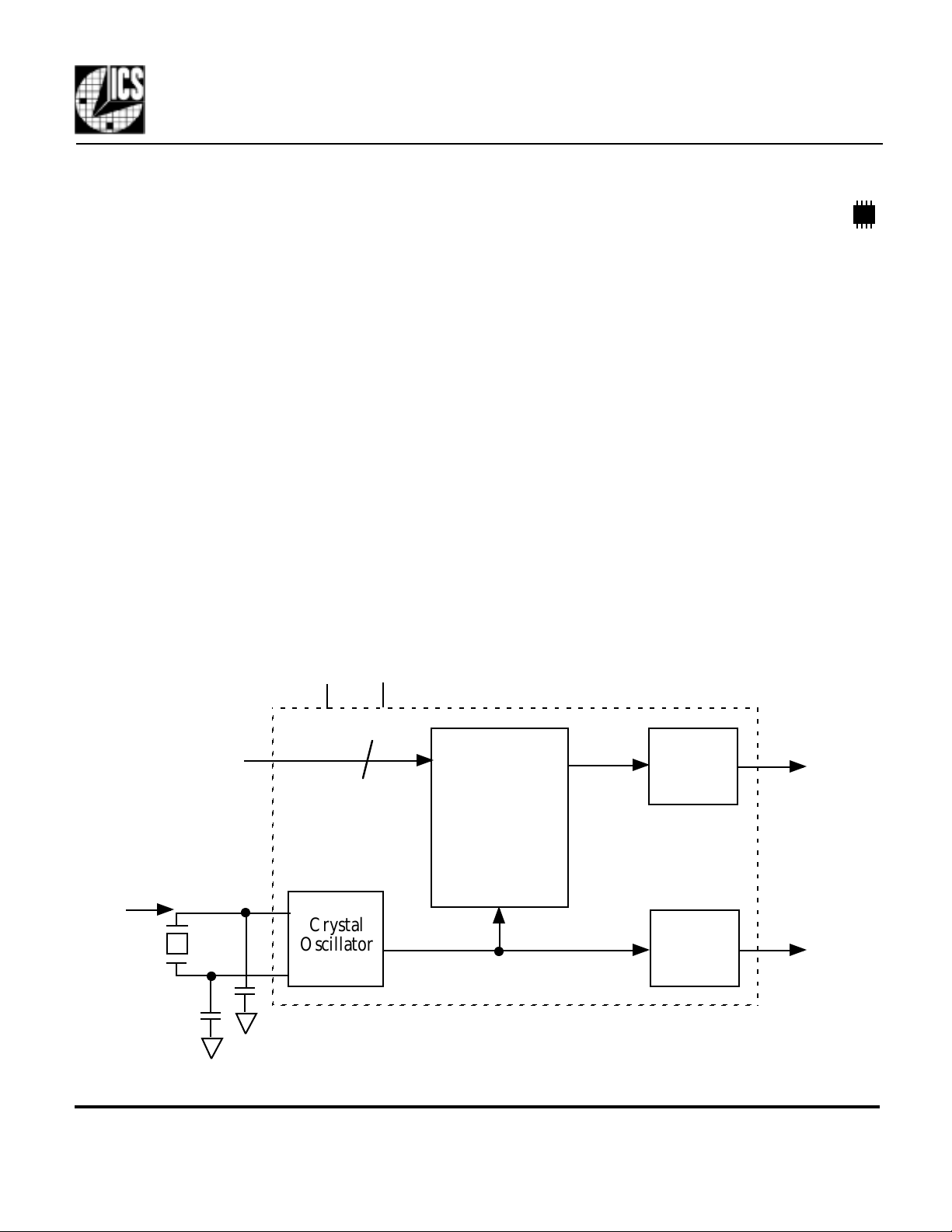
Block Diagram
Features
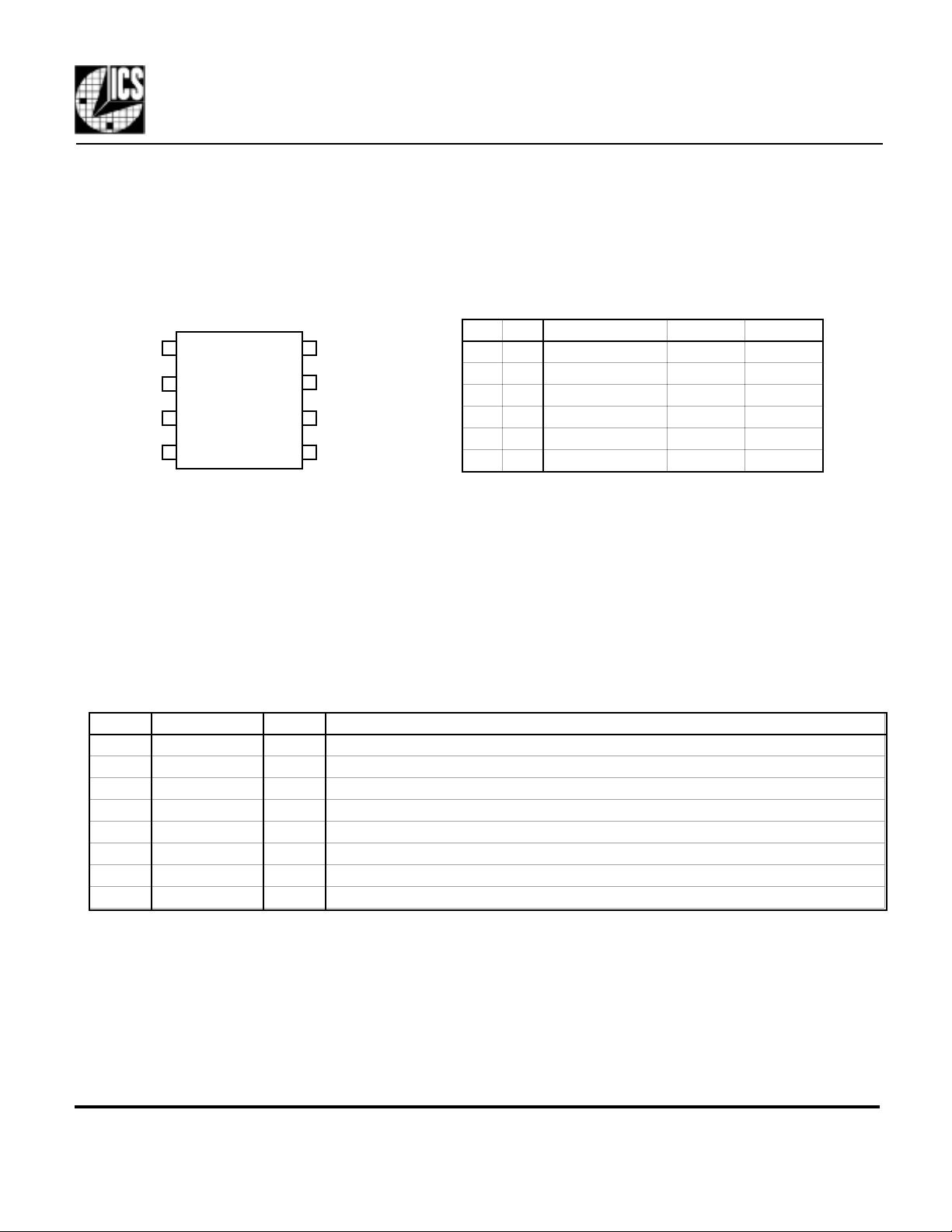
• Packaged as 8 pin SOIC
• ICS’ lowest cost PLL clock plus reference
• Produces common computer frequencies
• Input crystal frequency typically 14.3182 MHz
• Output clock frequencies up to 66.66 MHz
• Low jitter - 40 ps one sigma
• Compatible with all popular CPUs
• Duty cycle of 45/55
• Custom frequencies available
• Operating voltages of 3.0 to 5.5 V
• Power down mode turns off chip
• 25mA drive capability at TTL levels
• Advanced, low power CMOS process
14.31818 MHz
crystal or clock
X1/ICLK
X2
S1, S0
VDD GND
2
Crystal
Oscillator
Optional crystal capacitors
PLL
Clock
Synthesis
and Control
Circuitry
Output
Buffer
Output
Buffer
CLK
REF
MDS 514 B 1Revision 080699 Printed 11/13/00
Integrated Circuit Systems • 525 Race Street • San Jose•CA • 95126 • (408)295-9800tel• (408)295-9818fax
ICS514
p
p
LOCO™ PLL Clock Generator
Pin Assignment
X1/ICLK
VDD
GND
REF
18
2
3
4
X2
7
S1
6
S0
5
CLK
14.31818MHz Crystal or Clock Input
S1 S0 CLK Multiplier Accuracy
0 0 Power Down CLK - -
0 1 25 1.746 1 ppm
M 0 33.33 2.328 0.008%
M 1 40 2.794 1 ppm
1 0 50 3.492 1 ppm
1 1 66.66 4.656 0.008%
0 = connect directly to ground.
1 = connect directly to VDD.
M = leave unconnected (floating).
CLK and REF sto
low in power down state.
Pin Descriptions
Number Name Type Description
1 X1/ICLK I Crystal connection to 14.31818 MHz crystal or clock input.
2 VDD P Connect to +3.3V or +5V.
3 GND P Connect to ground.
4 REF O Reference 14.31818 MHz crystal oscillator buffered clock output.
5 CLK O Clock output per table above.
6 S0 TI Select 0 for output clock. Connect to GND or VDD or float. See table above.
7 S1 TI Select 1 for output clock. Connect to GND or VDD or float. See table above.
8 X2 O Crystal connection to 14.31818 MHz crystal. Leave unconnected for clock input.
Clock Decoding Table (MHz) with
Key: I = Input, TI = Tri-Level Input, O = output, P = power supply connection
Notes: 1. With S1 = S0 = 0, the internal PLL is turned off and the CLK output stops low.
The crystal oscillator and REF output are still active.
2. With a clock input, the phase relationship between the input and output clocks can
change each time the device is powered on. If a fixed phase relationship is required,
lease use our ICS571 or other zero delay multipliers.
MDS 514 B 2Revision 080699 Printed 11/13/00
Integrated Circuit Systems • 525 Race Street • San Jose•CA • 95126 • (408)295-9800tel• (408)295-9818fax
 Loading...